max7219.docx
《max7219.docx》由会员分享,可在线阅读,更多相关《max7219.docx(61页珍藏版)》请在冰豆网上搜索。
max7219
_______________GeneralDescription
TheMAX7219/MAX7221arecompact,serialinput/out-
putcommon-cathodedisplaydriversthatinterface
microprocessors(µPs)to7-segmentnumericLEDdis-
playsofupto8digits,bar-graphdisplays,or64indi-
vidualLEDs.Includedon-chipareaBCDcode-B
decoder,multiplexscancircuitry,segmentanddigit
drivers,andan8x8staticRAMthatstoreseachdigit.
Onlyoneexternalresistorisrequiredtosettheseg-
mentcurrentforallLEDs.TheMAX7221iscompatible
withSPI™,QSPI™,andMicrowire™,andhasslew-rate-
limitedsegmentdriverstoreduceEMI.
Aconvenient3-wireserialinterfaceconnectstoall
commonµPs.Individualdigitsmaybeaddressedand
updatedwithoutrewritingtheentiredisplay.The
MAX7219/MAX7221alsoallowtheusertoselectcode-
Bdecodingorno-decodeforeachdigit.
Thedevicesincludea150µAlow-powershutdown
mode,analoganddigitalbrightnesscontrol,ascan-
limitregisterthatallowstheusertodisplayfrom1to8
digits,andatestmodethatforcesallLEDson.
________________________Applications
Bar-GraphDisplays
7-SegmentDisplays
IndustrialControllers
PanelMeters
LEDMatrixDisplays
____________________________Features
o10MHzSerialInterface
oIndividualLEDSegmentControl
oDecode/No-DecodeDigitSelection
o150µALow-PowerShutdown(DataRetained)
oDigitalandAnalogBrightnessControl
oDisplayBlankedonPower-Up
oDriveCommon-CathodeLEDDisplay
oSlew-RateLimitedSegmentDrivers
forLowerEMI(MAX7221)
oSPI,QSPI,MicrowireSerialInterface(MAX7221)
o24-PinDIPandSOPackages
SeriallyInterfaced,8-DigitLEDDisplayDrivers
________________________________________________________________MaximIntegratedProducts1
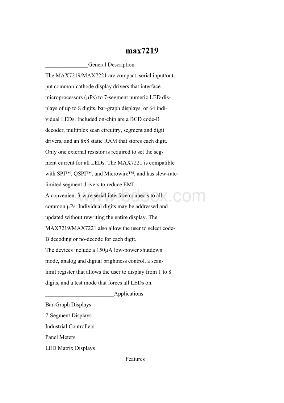
()MAX7221ONLY
8-DIGIT∝PDISPLAY
DIG0–DIG7
MOSI
I/O
SCK
18
1
12
13
9
4
DIN
∝P
ISET
9.53k
8DIGITS
8SEGMENTS
+5V
19
SEGA–G,
SEGDP
CLK
LOAD(CS)
GND
V+
GND
MAX7219
MAX7221
________TypicalApplicationCircuit
__________________PinConfiguration
24
23
22
21
20
19
18
17
1
2
3
4
5
6
7
8
DOUT
SEGD
SEGDP
SEGE
GND
DIG4
DIG0
DIN
TOPVIEW
SEGC
V+
ISET
SEGG
DIG7
DIG3
DIG2
DIG6
16
15
14
13
9
10
11
12
SEGB
SEGF
SEGA
CLK
()MAX7221ONLY
LOAD(CS)
DIG1
DIG5
GND
DIP/SO
MAX7219
MAX7221
19-4452;Rev3;7/97
PART
MAX7219CNG
MAX7219CWG
MAX7219C/D
0°Cto+70°C
0°Cto+70°C
0°Cto+70°C
TEMP.RANGEPIN-PACKAGE
24NarrowPlasticDIP
24WideSO
Dice*
______________OrderingInformation
OrderingInformationcontinuedatendofdatasheet.
*DicearespecifiedatTA=+25°C.
MAX7219ENG
MAX7219EWG
MAX7219ERG-40°Cto+85°C
-40°Cto+85°C
-40°Cto+85°C24NarrowPlasticDIP
24WideSO
24NarrowCERDIP
SPIandQSPIaretrademarksofMotorolaInc.MicrowireisatrademarkofNationalSemiconductorCorp.
Forfreesamples&thelatestliterature:
http:
//www.maxim-,orphone1-800-998-8800.
Forsmallorders,phone408-737-7600ext.3468.
MAX7219/MAX7221
SeriallyInterfaced,8-DigitLEDDisplayDrivers
2_______________________________________________________________________________________
ABSOLUTEMAXIMUMRATINGS
ELECTRICALCHARACTERISTICS
(V+=5V±10%,RSET=9.53kΩ±1%,TA=TMINtoTMAX,unlessotherwisenoted.)
Stressesbeyondthoselistedunder“AbsoluteMaximumRatings”maycausepermanentdamagetothedevice.Thesearestressratingsonly,andfunctional
operationofthedeviceattheseoranyotherconditionsbeyondthoseindicatedintheoperationalsectionsofthespecificationsisnotimplied.Exposureto
absolutemaximumratingconditionsforextendedperiodsmayaffectdevicereliability.
Voltage(withrespecttoGND)
V+............................................................................-0.3Vto6V
DIN,CLK,LOAD,CS...............................................-0.3Vto6V
AllOtherPins.............................................-0.3Vto(V++0.3V)
Current
DIG0–DIG7SinkCurrent................................................500mA
SEGA–G,DPSourceCurrent.........................................100mA
ContinuousPowerDissipation(TA=+85°C)
NarrowPlasticDIP..........................................................0.87W
WideSO..........................................................................0.76W
NarrowCERDIP.................................................................1.1W
OperatingTemperatureRanges
MAX7219C_G/MAX7221C_G..............................0°Cto+70°C
MAX7219E_G/MAX7221E_G............................-40°Cto+85°C
StorageTemperatureRange.............................-65°Cto+160°C
LeadTemperature(soldering,10sec).............................+300°C
RSET=opencircuit
AlldigitalinputsatV+orGND,TA=+25°C
Digitoff,VDIGIT=V+
TA=+25°C,V+=5V,VOUT=(V+-1V)
Allsegmentsanddecimalpointon,
ISEG_=-40mA
8digitsscanned
V+=5V,VOUT=0.65V
TA=+25°C,V+=5V,VOUT=(V+-1V)
CONDITIONS
8
OperatingSupplyCurrent
µA
150
I+
V
4.0
5.5
V+
OperatingSupplyVoltage
ShutdownSupplyCurrent
µA
-10
IDIGIT
DigitDriveLeakage
(MAX7221only)
%
3.0
∆ISEGSegmentDriveCurrentMatching
mA/µs
10
20
50
∆ISEG/∆t
SegmentCurrentSlewRate
(MAX7221only)
mA
330
I+
Hz
500
8001300
fOSC
DisplayScanRate
mA
320
IDIGIT
DigitDriveSinkCurrent
mA
-30
-40
-45
ISEG
SegmentDriveSourceCurrent
UNITS
MINTYPMAX
SYMBOL
PARAMETER
Segmentoff,VSEG=0V
µA
1
ISEG
SegmentDriveLeakage
(MAX7221only)
Digitoff,VDIGIT=(V+-0.3V)
mA
-2
IDIGIT
DigitDriveSourceCurrent
(MAX7219only)
Segmentoff,VSEG=0.3V
mA
5
ISEG
SegmentDriveSinkCurrent
(MAX7219only)
MAX7219/MAX7221
SeriallyInterfaced,8-DigitLEDDisplayDrivers
_______________________________________________________________________________________3
ELECTRICALCHARACTERISTICS(continued)
(V+=5V±10%,RSET=9.53kΩ±1%,TA=TMINtoTMAX,unlessotherwisenoted.)
VIN=0VorV+
DOUT,ISINK=1.6mA
DOUT,ISOURCE=-1mA
CONDITIONS
µA
-1
1
IIH,IIL
InputCurrentDIN,CLK,
LOAD,CS
V
0.4
VOL
OutputLowVoltage
V
3.5
VIH
LogicHighInputVoltage
V
0.8
VIL
LogicLowInputVoltage
V
V+-1
VOH
OutputHighVoltage
UNITS
MINTYPMAX
SYMBOL
PARAMETER
DIN,CLK,LOAD,CS
V
1
∆VI
HysteresisVoltage
ns
25
tCSS
CSFalltoSCLKRiseSetupTime
(MAX7221only)
ns
100
tCP
CLKClockPeriod
ns
50
tCH
CLKPulseWidthHigh
ns
50
tCL
CLKPulseWidthLow
CLOAD=50pF
ns
25
tDS
DINSetupTime
ns
50
tCSW
MinimumCSorLOADPulse
High
ns
0
tDH
DINHoldTime
ns
25
tDO
OutputDataPropagationDelay
ns
50
tLDCK
Load-RisingEdgetoNextClock
RisingEdge(MAX7219only)
ns
0
tCSH
CLKRisetoCSorLOADRise
HoldTime
ms
2.25
tDSPD
Data-to-SegmentDelay
LOGICINPUTS
TIMINGCHARACTERISTICS
MAX7219/MAX7221
SeriallyInterfaced,8-DigitLEDDisplayDrivers
4_______________________________________________________________________________________
__________________________________________TypicalOperatingCharacteristics
(V+=+5V,TA=+25°C,unlessotherwisenoted.)
730
750
740
770
760
790
780
800
820
810
830
4.04.44.85.25.66.0
SCANFREQUENCYvs.
POSITIVESUPPLYVOLTAGE
POSITIVESUPPLYVOLTAGE(V)
0
20
10
40
30
60
50
70
01
2
34
5
SEGMENTDRIVEROUTPUTCURRENT
vs.OUTPUTVOLTAGE
OUTPUTVOLTAGE(V)
RSET=10kΩ
RSET=20kΩ
RSET=40kΩ
MAX7219
SEGMENTOUTPUTCURRENT
5∝s/div
10mA/div
0
MAXIMUMINTENSITY=31/32
MAX7221
SEGMENTOUTPUTCURRENT
5∝s/div
10mA/div
0
MAXIMUMINTENSITY=15/16
MAX7219/MAX7221
MAX7219/2101
SCANFREQUENCY(Hz)
MAX7219/2102
OUTPUTCURRENT(mA)
MAX7219/2103
MAX7219/2104
SeriallyInterfaced,8-DigitLEDDisplayDrivers
_______________________________________________________________________________________5
______________________________________________________________PinDescription
_________________________________________________________FunctionalDiagram
NAME
FUNCTION
1
DIN
Serial-DataInput.Dataisloadedintotheinternal16-bitshiftregisteronCLK’srisingedge.
2,3,5–8,
10,11
DIG0–DIG7
Eight-DigitDriveLinesthatsinkcurrentfromthedisplaycommoncathode.TheMAX7219pulls
thedigitoutputstoV+whenturnedoff.TheMAX7221’sdigitdriversarehigh-impedancewhen
turnedoff.
PIN
4,9
GND
Ground(bothGNDpinsmustbeconnected)
12
LOAD
(MAX7219)
18
ISET
ConnecttoVDDthrougharesistor(RSET)tosetthepeaksegmentcurrent(RefertoSelecting
RSETResistorsection).
14–17,
20–23
SEGA–SEGG,
DP
13
CLK
CS
(MAX7221)
24
DOUT
Serial-DataOutput.ThedataintoDINisvalidatDOUT16.5clockcycleslater.Thispinisused
todaisy-chainseveralMAX7219/MAX7221’sandisneverhigh-impedance.
19
V+
PositiveSupplyVoltage.Connectto+5V.
()MAX7221ONLY
V+
8
8
8
8
4
RSET
LOAD(CS)
DIN
DOUT
CLK
(MSB)
(LSB)
D0
SEGA–SEGG,DP
DIG0–DIG7
SHUTDOWNREGISTER
MODEREGISTER
INTENSITYREGISTER
SCAN-LIMITREGISTER
DISPLAY-TESTREGISTER
INTENSITY
PULSE-
WIDTH
MODULATOR
MULTIPLEX
SCAN
CIRCUITRY
ADDRESS
REGISTER
DECODER
8x8
DUAL-PORT
SRAM
8
D1D2D3D4D5D6D7D8D9D10D11D12
DIGITDRIVERS
D13D14D15
CODEB
ROMWITH
BYPASS
SEGMENT
CURRENT
REFERENCE
SEGMENTDRIVERS
Load-DataInput.Thelast16bitsofserialdataarelatchedonLOAD’srisingedge.
Chip-SelectInput.SerialdataisloadedintotheshiftregisterwhileCSislow.Thelast16bitsof
serialdataarelatchedonCS’srisingedge.
Serial-ClockInput.10MHzmaximumrate.OnCLK’srisingedge,dataisshiftedintotheinter-
nalshiftregister.OnCLK’sfallingedge,dataisclockedoutofDOUT.OntheMAX7221,the
CLKinputisactiveonlywhileCSislow.
SevenSegmentDrivesandDecimalPointDrivethatsourcecurrenttothedisplay.Onthe
MAX7219,whenasegmentdriveristurnedoffitis
 升级会员
升级会员 