硅超大规模集成电路工艺技术理论实践与模型课后习题答案.docx
《硅超大规模集成电路工艺技术理论实践与模型课后习题答案.docx》由会员分享,可在线阅读,更多相关《硅超大规模集成电路工艺技术理论实践与模型课后习题答案.docx(40页珍藏版)》请在冰豆网上搜索。
硅超大规模集成电路工艺技术理论实践与模型课后习题答案
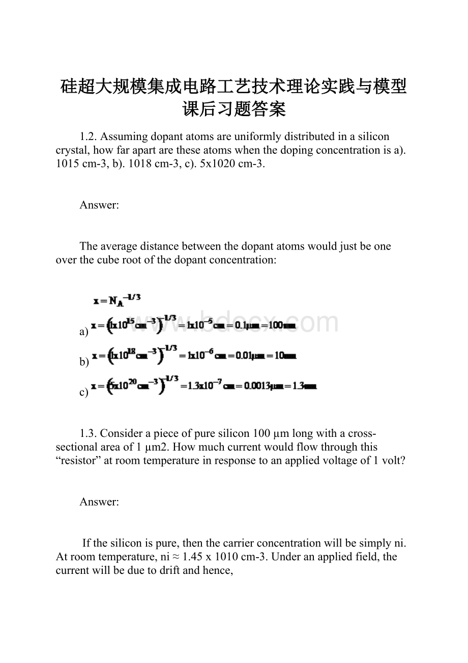
1.2.Assumingdopantatomsareuniformlydistributedinasiliconcrystal,howfarapartaretheseatomswhenthedopingconcentrationisa).1015cm-3,b).1018cm-3,c).5x1020cm-3.
Answer:
Theaveragedistancebetweenthedopantatomswouldjustbeoneoverthecuberootofthedopantconcentration:
a)
b)
c)
1.3.Considerapieceofpuresilicon100µmlongwithacross-sectionalareaof1µm2.Howmuchcurrentwouldflowthroughthis“resistor”atroomtemperatureinresponsetoanappliedvoltageof1volt?
Answer:
Ifthesiliconispure,thenthecarrierconcentrationwillbesimplyni.Atroomtemperature,ni≈1.45x1010cm-3.Underanappliedfield,thecurrentwillbeduetodriftandhence,
1.10.Astate-of-the-artNMOStransistormighthaveadrainjunctionareaof0.5x0.5µm.Calculatethejunctioncapacitanceassociatedwiththisjunctionatanappliedreversebiasof2volts.Assumethedrainregionisveryheavilydopedandthesubstratedopingis1x1016cm-3.
Answer:
ThecapacitanceofthejunctionisgivenbyEqn.1.25.
Thejunctionbuilt-involtageisgivenbyEqn.1.24.NDisnotspecifiedexceptthatitisverylarge,sowetakeittobe1020cm-3(roughlysolidsolubility).TheexactchoiceforNDdoesn'tmakemuchdifferenceintheanswer.
SinceND>>NAinthisstructure,thecapacitanceexpressionsimplifiesto
Giventheareaofthejunction(0.25x10⁻⁸cm2,thejunctioncapacitanceisthus4.2x10-17Farads.
3.2.Aboron-dopedcrystalpulledbytheCzochralskitechniqueisrequiredtohavearesistivityof10Ωcmwhenhalfthecrystalisgrown.Assumingthata100gmpuresiliconchargeisused,howmuch0.01Ωcmborondopedsiliconmustbeaddedtothemelt?
Forthiscrystal,plotresistivityasafunctionofthefractionofthemeltsolidified.Assumek0=0.8andtheholemobilityµp=550cm2volt-1sec-1.
Answer:
Usingthemobilityvaluegiven,and
wehave:
10Ωcm⇒NA=1.14x1015cm-3and0.01Ωcm⇒NA=1.14x1018cm-3
FromEqn.3.38,
andwewantCS=1.14x1015cm-3whenf=0.5.Thus,solvingforC0theinitialdopingconcentrationinthemelt,wehave:
Theresistivityasafunctionofdistanceisplottedbelowandisgivenby
3.3.ACzochralskicrystalispulledfromameltcontaining1015cm-3boronand2x1014cm-3phosphorus.InitiallythecrystalwillbePtypebutasitispulled,moreandmorephosphoruswillbuildupintheliquidbecauseofsegregation.AtsomepointthecrystalwillbecomeNtype.AssumingkO=0.32forphosphorusand0.8forboron,calculatethedistancealongthepulledcrystalatwhichthetransitionfromPtoNtypetakesplace.
Answer:
WecancalculatethepointatwhichthecrystalbecomesNtypefromEqn.3.38asfollows:
Atthepointwherethecross-overoccurstoNtype,thesetwoconcentrationswillbeequal.Solvingforf,wefind
Thusonlythelast0.5%ofthecrystalisNtype.
3.6.SupposeyourcompanywasinthebusinessofproducingsiliconwafersforthesemiconductorindustrybytheCZgrowthprocess.Supposeyouhadtoproducethemaximumnumberofwafersperboulethatmetafairlytightresistivityspecification.
a).WouldyouprefertogrowNtypeorPtypecrystals?
Why?
b).WhatdopantwouldyouuseingrowingN-typecrystals?
WhatdopantwouldyouuseingrowingPtypecrystals?
Explain
Answer:
a).Boronhasthesegregationcoefficientclosesttounityofallthedopants.ThusitproducesthemostuniformdopingalongthelengthofaCZcrystal.ThusPtypewouldbethenaturalchoice.
b).ForPtype,theobvious(andonlyrealchoice)isboronasexplainedinparta).ForNtypecrystalsFig.3-18showsthateitherPorAswouldbeareasonablechoicesincetheirsegregationcoefficientsarequitecloseandarebetterthanSb.Table3-2indicatesthatPmightbeslightlypreferredoverAsbecauseitskOvalueisslightlycloserto1.
4.1.AnICmanufacturingplantproduces1000wafersperweek.Assumethateachwafercontains100die,eachofwhichcanbesoldfor$50ifitworks.Theyieldonthesechipsiscurrentlyrunningat50%.Iftheyieldcanbeincreased,theincrementalincomeisalmostpureprofitbecauseall100chipsoneachwaferaremanufacturedwhethertheyworkornot.Howmuchwouldtheyieldhavetobeincreasedtoproduceanannualprofitincreaseof$10,000,000?
Answer:
At1000wafersperweek,theplantproduces52,000wafersperyear.Ifeachwaferhas50gooddieeachofwhichsellsfor$50,theplantgrossincomeissimply
Income=(52,000)(50)($50)=$130,000,000peryear.
Toincreasethisincomeby$10,000,000requiresthattheyieldincreaseby
4.3.AsMOSdevicesarescaledtosmallerdimensions,gateoxidesmustbereducedinthickness.
a.Asthegateoxidethicknessdecreases,doMOSdevicesbecomemoreorlesssensitivetosodiumcontamination?
Explain.
b.Asthegateoxidethicknessdecreases,whatmustbedonetothesubstratedoping(oralternativelythechannelVTHimplant,tomaintainthesameVTH?
Explain.
Answer:
a).Fromthetext,Na+contaminationcausesthresholdvoltageinstabilitiesinMOSdevices.AlsofromEqn.4.1,thethresholdvoltageisgivenby
Asthegateoxidethicknessdecreases,COXincreases,sothesameamountofmobilechargeQMwillhavelesseffectonVTHasoxidesgetthinner.ThereforeMOSdevicesarelesssensitivetosodiumcontamination.
b).UsingthesameexpressionforVTHasinparta),weobservethatastheoxidethicknessdecreases,(COXincreases),tomaintainthesameVTH,NAwillhavetoincrease.NAwillactuallyhavetoincreasebythesquarerootoftheoxidethicknessdecreasetokeepVTHconstant.
4.4.AnewcleaningprocedurehasbeenproposedwhichisbasedonH2OsaturatedwithO2asanoxidant.ThishasbeensuggestedasareplacementfortheH2O2oxidizingsolutionusedintheRCAclean.SupposeaSiwafer,contaminatedwithtraceamountsofAu,FeandCuiscleanedinthenewH2O/O2solution.Willthiscleanthewafereffectively?
Whyorwhynot?
Explain.
Answer:
Asdescribedinthetext,cleaningmetalionsoffofsiliconwafersinvolvesthefollowingchemistry:
Thecleaningsolutionmustbechosensothatthereactionisdriventotherightbecausethisputsthemetalionsinsolutionwheretheycanberinsedoff.Sincedrivingthereactiontotherightcorrespondstooxidation,weneedanoxidizingsolutiontocleanthewafer.
H2O/O2iscertainlyanoxidizingsolution.Butwhetheritcleanseffectivelyornotdependsonthestandardoxidationpotentialofthevariouspossiblereactions.FromTable4-3inthetext,wehave:
Oxidant/
Reductant
StandardOxidation
Potential(volts)
Oxidation-ReductionReaction
SiO2/Si
0.84
/Fe
0.17
/Cu
-0.34
/H2O
-1.23
/Au
-1.42
Thestrongerreactions(dominating)areatthebottom.
ThustheH2O/O2reactionwillcleanFeandCu,butitwillnotcleanAuoffthewafer.
4.5.ExplainwhyitisimportantthatthegenerationlifetimemeasurementillustratedinFigure4-19isdoneinthedark.
Answer:
Themeasurementdependsonmeasuringcarriersgeneratedthermallyinthesiliconsubstrate(oratthesurface).Iflightisshiningonthesample,thenabsorbedphotonscanalsogeneratetherequiredcarriers.Asaresult,theextractedgenerationlifetimewiththelightonwouldreallybemeasuringtheintensityoftheincidentlightandnotabasicpropertyofthesiliconmaterial.
5.1.CalculateandplotversusexposurewavelengththetheoreticalresolutionanddepthoffocusforaprojectionexposuresystemwithaNAof0.6(aboutthebestthatcanbedonetoday).Assumek1=0.6andk2=0.5(bothtypicalvalues).Considerwavelengthsbetween100nmand1000nm(DUVandvisiblelight).).Indicatethecommonexposurewavelengthsbeingusedorconsideredtodayonyourplot(g-line,i-line,KrFandArF).WillanArFsourcebeadequateforthe0.13µmand0.1µmtechnologygenerationsaccordingtothesesimplecalculations?
Answer:
Therelevantequationsaresimply
Theseequationsareplottedbelow.NotethattheArF(193nm)willnotreach0.13µmor0.1µmresolutionaccordingtothesesimplecalculations.Infact,withmoresophisticatedtechniquessuchasphaseshiftmasks,offaxisilluminationetc.,ArFisexpectedtoreach0.13µmandperhapsthe0.1µmgenerations.
5.3.AnX-rayexposuresystemusesphotonswithanenergyof1keV.Iftheseparationbetweenthemaskandwaferis20µm,estimatethediffractionlimitedresolutionthatisachievablebythissystem.
Answer:
Theequivalentwavelengthof1keVx-raysisgivenby
X-raysystemsoperateintheproximityprintingmode,sothatthetheoreticalresolutionisgivenbyEqn.5.12:
5.8.Asdescribedinthischapter,therearenoclearchoicesforlithographysystemsbeyondopticalprojectiontoolsbasedon193-nmArFeximerlasers.Onepossibilityisanopticalprojectionsystemusinga157-nmF2excimerlaser.
a.Assuminganumericalapertureof0.8andk1=0.75,whatistheexpectedresolutionofsuchasystemusingafirstorderestimateofresolution?
b.Actualprojectionsforsuchsystemssuggestthattheymightbecapableofresolvingfeaturessuitableforthe20090.07µmgeneration.Suggestthreeapproachestoactuallyachievingthisresolutionwiththesesystems.
Answer
a).Thesimpleformulaforresolutionis
b).Thecalculatedresolutioninpartaisafactoroftwolargerthanrequiredforthe0.07µmgeneration.Thereforesome“tricks”willhavetobeusedtoactuallyachievesuchres
 升级会员
升级会员 