Microchip dsPIC33FJ PSFB砖形DCDC转换器参考设计.docx
《Microchip dsPIC33FJ PSFB砖形DCDC转换器参考设计.docx》由会员分享,可在线阅读,更多相关《Microchip dsPIC33FJ PSFB砖形DCDC转换器参考设计.docx(20页珍藏版)》请在冰豆网上搜索。
MicrochipdsPIC33FJPSFB砖形DCDC转换器参考设计
MicrochipdsPIC33FJPSFB砖形DC-DC转换器参考设计
关键词:
电源管理,DC/DC转换器
Microchip公司的dsPIC33FJ06GS101/X02和dsPIC33FJ16GSX02/X04包括有广泛的DSP功能和高性能16位MCU架构。
3.0-3.6V的性能达到40MIPS,具有16位宽的数据通路,24位宽指令,广泛应用在AC/DC转换器,汽车HID,电池充电器,DC/DC转换器,数字照明,电磁炉,可再生能源/纯正弦波逆变器和UPS。
本文介绍了dsPIC33FJ系列主要特性,方框图和CPU核方框图,DSP引擎方框图,数字PFC框图以及多种应用框图。
此外还介绍了相移全桥(PSFB)1/4砖形DC-DC转换器参考设计主要特性和指标,详细电路图与材料清单(BOM)。
dsPIC33FJ06GS101/X02anddsPIC33FJ16GSX02/X04devicescontainextensiveDigitalSignalProcessor(DSP)functionalitywithahigh-performance,16-bitmicrocontroller(MCU)architecture.
dsPIC33FJ系列主要特性:
OperatingRange:
•Upto40MIPSOperation(at3.0-3.6V):
-Industrialtemperaturerange(-40℃to+85℃)
-Extendedtemperaturerange(-40℃to+125℃)
High-PerformanceDSCCPU:
•ModifiedHarvardArchitecture
•CCompilerOptimizedInstructionSet
•16-BitWideDataPath
•24-BitWideInstructions
•LinearProgramMemoryAddressingupto4MInstructionWords
•LinearDataMemoryAddressingupto64Kbytes
•83BaseInstructions:
Mostly1Word/1Cycle
•Two40-BitAccumulatorswithRoundingandSaturationOptions
•FlexibleandPowerfulAddressingmodes:
-Indirect
-Modulo
-Bit-Reversed
•SoftwareStack
•16x16Fractional/IntegerMultiplyOperations
•32/16and16/16DivideOperations
•Single-CycleMultiplyandAccumulate:
-AccumulatorwritebackforDSPoperations
-Dualdatafetch
•Upto±16-BitShiftsforupto40-BitData
DigitalI/O:
•PeripheralPinSelectFunctionality
•Upto35ProgrammableDigitalI/OPins
•Wake-up/Interrupt-on-Changeforupto30Pins
•OutputPinscanDriveVoltagefrom3.0Vto3.6V
•Upto5VOutputwithOpen-DrainConfiguration
•5VTolerantDigitalInputPins(exceptRB5)
•16mASource/SinkonAllPWMpins
On-ChipFlashandSRAM:
•FlashProgramMemory(upto16Kbytes)
•DataSRAM(upto2Kbytes)
•BootandGeneralSecurityforProgramFlash
PeripheralFeatures:
•Timer/Counters,uptoThree16-BitTimers:
-Canpairuptomakeone32-bittimer
•InputCapture(uptotwochannels):
-Captureonup,downorbothedges
-16-bitcaptureinputfunctions
-4-deepFIFOoneachcapture
•OutputCompare(uptotwochannels):
-SingleorDual16-BitComparemode
-16-BitGlitchlessPWMmode
•4-WireSPI:
-FramingsupportsI/Ointerfacetosimplecodecs
-1-deepFIFOBuffer.
-Supports8-bitand16-bitdata
-Supportsallserialclockformatsandsamplingmodes
•I2C™:
-SupportsFullMulti-MasterSlavemode
-7-bitand10-bitaddressing
-Buscollisiondetectionandarbitration
-Integratedsignalconditioning
-Slaveaddressmasking
•UART:
-Interruptonaddressbitdetect
-InterruptonUARTerror
-Wake-uponStartbitfromSleepmode
-4-characterTXandRXFIFObuffers
-LINbussupport
-IrDA®encodinganddecodinginhardware
-High-SpeedBaudmode
-HardwareFlowControlwithCTSandRTS
InterruptController:
•5-CycleLatency
•Upto35AvailableInterruptSources
•UptoThreeExternalInterrupts
•SevenProgrammablePriorityLevels
•FourProcessorExceptions
High-SpeedPWMModuleFeatures:
•UptoFourPWMGeneratorswithFourtoEightOutputs
•IndividualTimeBaseandDutyCycleforeachoftheEightPWMOutputs
•DeadTimeforRisingandFallingEdges
•DutyCycleResolutionof1.04ns
•Dead-TimeResolutionof1.04ns
•PhaseShiftResolutionof1.04ns
•FrequencyResolutionof1.04ns
•PWMmodesSupported:
-StandardEdge-Aligned
-TrueIndependentOutput
-Complementary
-Center-Aligned
-Push-Pull
-Multi-Phase
-VariablePhase
-FixedOff-Time
-CurrentReset
-Current-Limit
•IndependentFault/Current-LimitInputsfor8PWMOutputs
•OutputOverrideControl
•SpecialEventTrigger
•PWMCaptureFeature
•PrescalerforInputClock
•DualTriggerfromPWMtoADC
•PWMxL,PWMxHOutputPinSwapping
•PWM4H,PWM4LPinsRemappable
•On-the-FlyPWMFrequency,DutyCycleandPhaseShiftChanges
•DisablingofIndividualPWMGenerators
•Leading-EdgeBlanking(LEB)Functionality
High-SpeedAnalogComparator
•UptoFourAnalogComparators:
-20nsresponsetime
-10-bitDACforeachanalogcomparator
-DACOUTpintoprovideDACoutput
-Programmableoutputpolarity
-Selectableinputsource
-ADCsampleandconvertcapability
•PWMModuleInterface:
-PWMdutycyclecontrol
-PWMperiodcontrol
-PWMFaultdetect
High-Speed10-BitADC
•10-BitResolution
•Upto12InputChannelsGroupedintoSixConversionPairs
•TwoInternalReferenceMonitoringInputsGroupedintoaPair
•SuccessiveApproximationRegister(SAR)
ConvertersforParallelConversionsofAnalogPairs:
-4MspsfordeviceswithtwoSARs
-2MspsfordeviceswithoneSAR
•DedicatedResultBufferforeachAnalogChannel
•IndependentTriggerSourceSectionforeachAnalogInputConversionPair
PowerManagement:
•On-Chip2.5VVoltageRegulator
•SwitchbetweenClockSourcesinRealTime
•Idle,Sleep,andDozemodeswithFastWake-up
CMOSFlashTechnology:
•Low-Power,High-SpeedFlashTechnology
•FullyStaticDesign
•3.3V(±10%)OperatingVoltage
•IndustrialandExtendedTemperature
•Low-PowerConsumption
SystemManagement:
•FlexibleClockOptions:
-External,crystal,resonator,internalRC
-Phase-LockedLoop(PLL)with120MHzVCO
-PrimaryCrystalOscillator(OSC)intherangeof3MHzto40MHz
-InternalLow-PowerRC(LPRC)oscillatoratafrequencyof32kHz
-InternalFastRC(FRC)oscillatoratafrequencyof7.37MHz
•Power-onReset(POR)
•Brown-outReset(BOR)
•Power-upTimer(PWRT)
•OscillatorStart-upTimer(OST)
•WatchdogTimerwithitsRCOscillator
•Fail-SafeClockMonitor(FSCM)
•ResetbyMultipleSources
•In-CircuitSerialProgramming™(ICSP™)
•ReferenceOscillatorOutput
dsPIC33FJ系列应用:
•AC-to-DCConverters
•AutomotiveHID
•BatteryChargers
•DC-to-DCConverters
•DigitalLighting
•InductionCooking
•LEDBallast
•RenewablePower/PureSineWaveInverters
•UninterruptiblePowerSupply(UPS)
图1。
dsPIC33FJ06GS101/X02和dsPIC33FJ16GSX02/X04方框图
图2。
dsPIC33FJ06GS101/X02和dsPIC33FJ16GSX02/X04CPU核方框图
图3。
DSP引擎方框图
图4。
dsPIC33FJ数字PFC框图
图5。
dsPIC33FJ升压转换器框图
图6。
dsPIC33FJ单相同步降压转换器框图
图7。
dsPIC33FJ多相同步降压转换器框图
图8。
dsPIC33FJ离线UPS框图
图9。
dsPIC33FJ交叉PFC框图
图10。
dsPIC33FJ相移全桥(PSFB)转换器框图
图11。
带PFC三输出(12V,5V和3.3V)AC/DC电源框图
1/4砖形DC/DC转换器参考设计
QuarterBrickDC/DCConverterReferenceDesign
Thisreferencedesignprovidesaneasymethodtoevaluatethepower,andfeaturesofSMPSdsPIC®DigitalSignalControllersinhighdensityquarterbrickDC-DCconvertersforintermediatebusarchitectures(IBA).ThisreferencedesignisimplementedusingasingledsPIC33F“GS”digital-powerDSCsfromMicrochipthatprovidesthefulldigitalcontrolofthepowerconversionandsystemmanagementfunctions.AsshowninthisreferencedesignthedsPIC33F‘GS’devicesenabledesignerstoeasilyandcosteffectivelycreateproductsusingadvancedswitchingtechniquessuchasPhaseShiftFullBridge(PSFB)topologythatlowerswitchinglossesandenableefficienciesashighas94%.TheQuarterbrickDC/DCConverterReferenceDesignisroyaltyfreewhenusedinaccordancewiththelicensingagreement.
Thisreferencedesignworkswithtelecominputrange36V–76VDCandprovides12Vwith200Wpower.Designedwithplanarmagnetics,thisreferencedesignimplementsvariousnon-lineartechniques,whichimprovestheperformanceandefficiency.
1/4砖形DC/DC转换器参考设计主要特性:
PrimaryandSecondaryMOSFETcontrol
ActiveCurrentShare
RemoteON/OFF
Programmablesoftstart
ControlledFalltime
Voltage,Current,Temperaturemonitoring&Protection
Configurableoutputvoltage
FullDigitalControl
1/4砖形DC/DC转换器参考设计指标:
IndustrystandardQuarter-brick(36.8x58.4x11.4mm)
Wideinputrange36V-76V
OutputVoltage:
12V
OutputCurrent:
17A
OutputPower:
200W
Efficiencygreaterthan93%
1500Vdcinputtooutputisolation
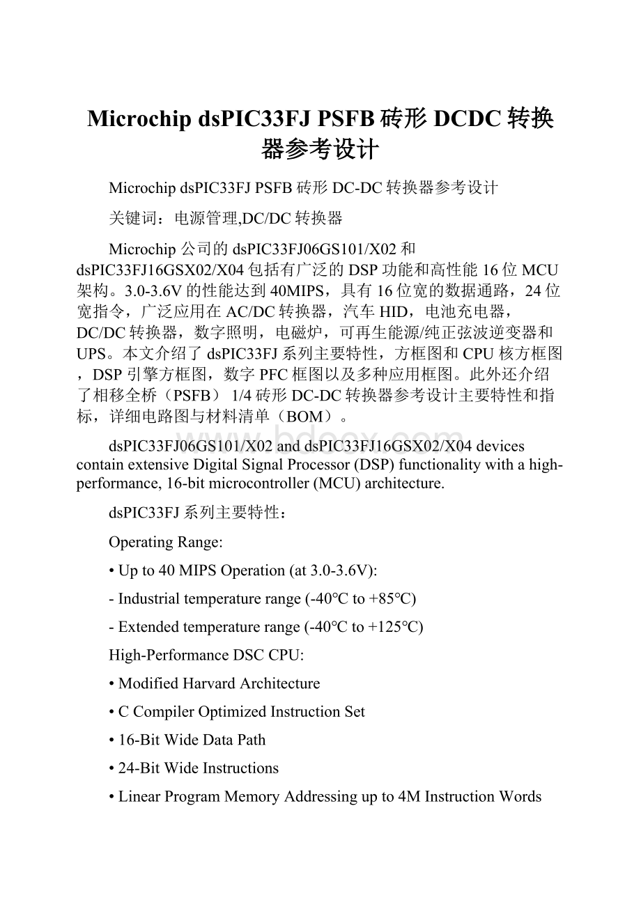
图12。
1/4砖形DC/DC转换器参考设计外形图
图13。
1/4砖形DC/DC转换器的dsPIC®DSC资源图
图14。
PSFB1/4砖形DC/DC转换器电路图
(1)
图15。
PSFB1/4砖形DC/DC转换器电路图
(2)
图16。
PSFB1/4砖形DC/DC转换器电路图(3)
图17。
PSFB1/4砖形DC/DC转换器电路图(4)
AO-Electronics傲壹电子官网:
中文网:
图18。
基板电路图
 升级会员
升级会员 