DRAM1Word文件下载.docx
《DRAM1Word文件下载.docx》由会员分享,可在线阅读,更多相关《DRAM1Word文件下载.docx(17页珍藏版)》请在冰豆网上搜索。
andother
static
memory.
Themainmemory(the"
RAM"
)inpersonalcomputersisDynamicRAM(DRAM),asisthe"
ofhomegameconsoles(PlayStation,Xbox360
and
Wii),
laptop,
notebook
workstation
computers.
TheadvantageofDRAMisitsstructuralsimplicity:
onlyonetransistorandacapacitorarerequiredperbit,comparedtosixtransistorsinSRAM.ThisallowsDRAMtoreachveryhigh
densities.Unlike
flashmemory,DRAMis
volatilememory
(cf.
non-volatilememory),sinceitlosesitsdataquicklywhenpowerisremoved.Thetransistorsandcapacitorsusedareextremelysmall;
hundredsofbillionscanfitonasinglememorychip.
History
The
cryptanalytic
machinecode-named
"
Aquarius"
usedat
BletchleyPark
during
WorldWarII
incorporatedahard-wireddynamicmemory.Papertapewasreadandthecharactersonit"
wererememberedinadynamicstore....Thestoreusedalargebankofcapacitors,whichwereeitherchargedornot,achargedcapacitorrepresentingcross
(1)andanunchargedcapacitordot(0).Sincethechargegraduallyleakedaway,aperiodicpulsewasappliedtotopupthosestillcharged(hencetheterm'
dynamic'
)"
.[1]
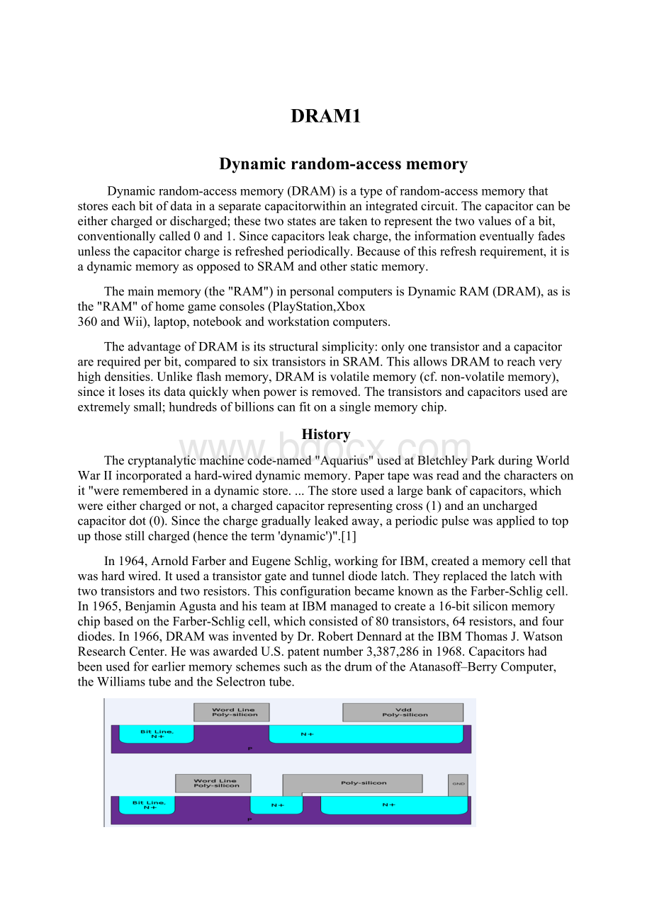
In1964,ArnoldFarberandEugeneSchlig,workingforIBM,createdamemorycellthatwashardwired.Itusedatransistorgateandtunneldiodelatch.Theyreplacedthelatchwithtwotransistorsandtworesistors.ThisconfigurationbecameknownastheFarber-Schligcell.In1965,BenjaminAgustaandhisteamatIBMmanagedtocreatea16-bitsiliconmemorychipbasedontheFarber-Schligcell,whichconsistedof80transistors,64resistors,andfourdiodes.In1966,DRAMwasinventedbyDr.
RobertDennard
atthe
IBM
ThomasJ.WatsonResearchCenter.HewasawardedU.S.patentnumber
3,387,286
in1968.Capacitorshadbeenusedforearliermemoryschemessuchasthedrumofthe
Atanasoff–BerryComputer,the
Williamstube
andthe
Selectrontube.
SchematicdrawingoforiginaldesignsofDRAMpatentedin1968.
ThefirstDRAMwithmultiplexedrowandcolumnaddresslineswasthe
Mostek
MK4096(4096x1)designedby
RobertProebsting
andintroducedin1973.Thisaddressingscheme,aradicaladvance,enabledittofitintopackageswithfewerpins,acostadvantagethatwouldgrowwitheveryjumpinmemorysize.TheMK4096provedtobeaveryrobustdesignforcustomerapplications.Atthe16Kdensity,thecostadvantageincreased,andtheMostekMK411616KDRAM,introducedin1976,achievedgreaterthan75%worldwideDRAMmarketshare.However,asdensityincreasedto64Kintheearly80s,MostekwasovertakenbyJapaneseDRAMmanufacturerssellinghigherqualityDRAMsusingthesamemultiplexingschemeatbelow-costprices.
Operationprinciple
DRAMisusuallyarrangedinasquarearrayofonecapacitorandtransistorperdatabitstoragecell.Theillustrationstotherightshowasimpleexamplewithonly4by4cells(ModernDRAMmatrixaremanythousandsofcellsinheightandwidth).
PrincipleofoperationofDRAMread,forsimple4by4array.
PrincipleofoperationofDRAMwrite,forsimple4by4array.
Toreadabitfromacolumn,thefollowingoperationstakeplace:
1.Thesenseamplifierisdisconnected,thenthebitlinesareprechargedtoexactlyequalvoltagesthatarein-betweenhighandlowlogiclevels.Thebitlinesarephysicallysymmetricaltokeepthecapacitanceasequalandthereforethevoltagesasequalaspossible.
2.Theprechargecircuitisswitchedoff.Becausethebitlinesarerelativelylong,theyhaveenoughcapacitance
tomaintainthepre-chargedvoltageforabrieftime.Thisisanexampleof
dynamiclogic.
3.Thedesiredrow'
swordlineisthendrivenhightoconnectacell'
sstoragecapacitortoitsbitline.Thiscausesthetransistortoconduct,transferring
charge
betweenthestoragecellandtheconnectedbitline.Ifthestoragecellcapacitorisdischarged,itwillgreatlydecreasethevoltageonthebit-lineastheprechargeistransferredtothestoragecapacitor.Ifthestoragecellischarged,thebit-linevoltagedecreasesonlyslightly;
thisbecauseeveryeffortismadetokeepthecapacitanceofthestoragecellshighandthecapacitanceofthebitlineslow.
4.Thesenseamplifierisswitchedon.Thepositivefeedbacktakesoverandamplifiesthesmallvoltagedifferencebetweenbit-linesuntilonebitlineisfullyatthelowestvoltageandtheotherisatthemaximumhighvoltage.Oncethishashappened,therowis"
open"
(thedesiredcelldataisavailable).
5.Allcolumnsaresensedinsimultaneouslyandtheresultsampledintothedatalatch.AprovidedColumnaddressthenselectswhichlatchbittoconnecttotheexternalcircuit.Manyreadscanbeperformedquicklywithoutdelaysensefortheopenrow,alldatahasalreadybeensensedandlatched.
6.Whilereadingallcolumnsproceeds(thenormalanddesirablemethodbecauseitmostquicklyprovidesdata),currentisflowingbackupthebitlinesfromthesenseamplifierstothestoragecells.Thisreinforces(i.e."
refreshes"
)thechargeinthestoragecellbyincreasingthevoltageinthestoragecapacitorifitwaschargedtobeginwith,orbykeepingitdischargedifitwasempty.Notethatduetothelengthofthebitlinescreatingafairlylongpropagationdelayforthechargetobetransferred,thistakessignificanttimebeyondtheendofsenseamplification,andthusoverlapswithoneormorecolumnreads.
7.Whendonewiththereadingallthecolumnsinthecurrentrow,thewordlineisswitchedofftodisconnectthecellstoragecapacitors(therowis"
closed"
),thesenseamplifierisswitchedoff,andthebitlinesareprechargedagain.
Towritetomemory,therowisopenedandagivencolumn'
ssenseamplifieristemporarilyforcedtothedesiredhighorlowvoltagestate,thusitdrivesthebitlinetochargeordischargethecellstoragecapacitortothedesiredvalue.Duetopositivefeedback,theamplifierwillthenholditstableevenaftertheforcingisremoved.Duringawritetoaparticularcell,allthecolumnsinarowaresensedsimultaneouslyjustasinreading,asinglecolumn'
scellstoragecapacitorchargeischanged,andthentheentirerowiswrittenbackin,asillustratedinthefiguretotheright.
Typically,manufacturersspecifythateachrowmustbehaveitsstoragecellcapacitorsrefreshedevery64
msorless,asdefinedbythe
JEDEC
(FoundationfordevelopingSemiconductorStandards)standard.
Refreshlogic
isprovidedinaDRAMcontrollerwhichautomatestheperiodicrefresh,thatisnosoftwareorotherhardwarehastoperformit.Thismakesthecontroller'
slogiccircuitmorecomplicated,butthisdrawbackisoutweighedbythefactthatDRAMismuchcheaperperstoragecellandbecauseeachstoragecellisverysimple,DRAMhasmuchgreatercapacitypergeographicareathanSRAM.
Somesystemsrefresheveryrowinaburstofactivityinvolvingallrowsevery64
ms.Othersystemsrefreshonerowatatimestaggeredthroughoutthe64msinterval.Forexample,asystemwith213
=
8192rowswouldrequireastaggered
refreshrate
ofonerowevery7.8
µ
swhichis64
msdividedby8192rows.Afewreal-timesystemsrefreshaportionofmemoryatatimedeterminedbyanexternaltimerfunctionthatgovernstheoperationoftherestofasystem,suchasthe
verticalblankinginterval
thatoccursevery10–20
msinvideoequipment.Allmethodsrequiresomesortofcountertokeeptrackofwhichrowisthenexttoberefreshed.MostDRAMchipsincludethatcounter.Oldertypesrequireexternalrefreshlogictoholdthecounter.(Undersomeconditions,mostofthedatainDRAMcanberecoveredeveniftheDRAMhasnotbeenrefreshedforseveralminutes.
Memorytiming
TherearemanynumbersrequiredtodescribethetimingofDRAMoperation.HerearesomeexamplesfortwotiminggradesofasynchronousDRAM,fromadatasheetpublishedin1998:
[3]
50
ns"
60
Description
tRC
84
ns
104
Randomreadorwritecycletime(fromonefull/RAScycletoanother)
tRAC
Accesstime:
/RASlowtovaliddataout
tRCD
11
14
/RASlowto/CASlowtime
tRAS
/RASpulsewidth(minimum/RASlowtime)
tRP
30
40
/RASprechargetime(minimum/RAShightime)
tPC
20
25
Page-modereadorwritecycletime(/CASto/CAS)
tAA
Columnaddressvalidtovaliddataout(includesaddress
setuptime
before/CASlow)
tCAC
13
15
/CASlowtovaliddataout
tCAS
8
10
/CASlowpulsewidthminimum
Thus,thegenerallyquotednumberisthe/RASaccesstime.ThisisthetimetoreadarandombitfromaprechargedDRAMarray.Thetimetoreadadditionalbitsfromanopenpageismuchless.
WhensuchaRAMisaccessedbyclockedlogic,thetimesaregenerallyroundeduptothenearestclockcycle.Forexample,whenaccessedbya100
MHzstatemachine(i.e.a10
nsclock),the50
nsDRAMcanperformthefirstreadinfiveclockcycles,andadditionalreadswithinthesamepageeverytwoclockcycles.Thiswasgenerallydescribedas
5‐2‐2‐2"
timing,asburstsoffourreadswithinapagewerecommon.
Whendescribingsynchronousmemory,timingisdescribedbyclockcyclecountsseparatedbyhyphens.Thesenumbersrepresent
tCL‐tRCD‐tRP‐tRAS
inmultiplesoftheDRAMclockcycletime.Notethatth
 升级会员
升级会员 