TBFNG数据手册.pdf
《TBFNG数据手册.pdf》由会员分享,可在线阅读,更多相关《TBFNG数据手册.pdf(11页珍藏版)》请在冰豆网上搜索。
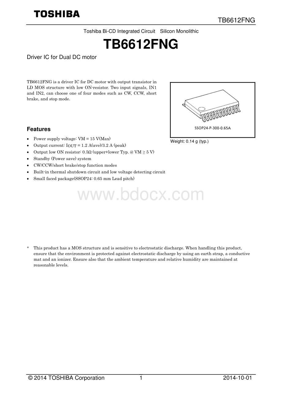
TB6612FNGToshibaBi-CDIntegratedCircuitSiliconMonolithicTB6612FNGDriverICforDualDCmotorTB6612FNGisadriverICforDCmotorwithoutputtransistorinLDMOSstructurewithlowON-resistor.Twoinputsignals,IN1andIN2,canchooseoneoffourmodessuchasCW,CCW,shortbrake,andstopmode.FeaturesPowersupplyvoltage:
VM=15V(Max)Outputcurrent:
IOUT=1.2A(ave)/3.2A(peak)OutputlowONresistor:
0.5(upper+lowerTyp.VM5V)Standby(Powersave)systemCW/CCW/shortbrake/stopfunctionmodesBuilt-inthermalshutdowncircuitandlowvoltagedetectingcircuitSmallfacedpackage(SSOP24:
0.65mmLeadpitch)*ThisproducthasaMOSstructureandissensitivetoelectrostaticdischarge.Whenhandlingthisproduct,ensurethattheenvironmentisprotectedagainstelectrostaticdischargebyusinganearthstrap,aconductivematandanionizer.Ensurealsothattheambienttemperatureandrelativehumidityaremaintainedatreasonablelevels.Weight:
0.14g(typ.)2014TOSHIBACorporation2014-10-011TB6612FNGBlockDiagramPinFunctionsNo.PinNameI/OFunction1AO1OchAoutput12AO13PGND1PowerGND14PGND15AO2OchAoutput26AO27BO2OchBoutput28BO29PGND2PowerGND210PGND211BO1OchBoutput112BO113VM2Motorsupply14VM315PWMBIchBPWMinput/200kpull-downatinternal16BIN2IchBinput2/200kpull-downatinternal17BIN1IchBinput1/200kpull-downatinternal18GNDSmallsignalGND19STBYI“L”=standby/200kpull-downatinternal20VccSmallsignalsupply21AIN1IchAinput1/200kpull-downatinternal22AIN2IchAinput2/200kpull-downatinternal23PWMAIchAPWMinput/200kpull-downatinternal24VM1Motorsupply2014-10-012TB6612FNGAbsoluteMaximumRatings(Ta=25C)OperatingRange(Ta=-20to85C)CharacteristicsSymbolRatingUnitRemarksSupplyvoltageVM15VVCC6InputvoltageVIN-0.2to6VIN1,IN2,STBY,PWMpinsOutputvoltageVOUT15VO1,O2pinsOutputcurrentIOUT1.2APer1chIOUT(peak)2tw=20msContinuouspulse,Duty20%3.2tw=10msSinglepulsePowerdissipationPD0.78WIConly0.8950mm50mmt=1.6mmCu40%inPCBmounting1.3676.2mm114.3mmt=1.6mmCu30%inPCBmountingOperatingtemperatureTopr-20to85CStoragetemperatureTstg-55to150CCharacteristicsSymbolMinTyp.MaxUnitRemarksSupplyvoltageVCC2.735.5VVM2.5513.5VOutputcurrent(H-SW)IOUT1.0AVM4.5V0.44.5VVM2.5VWithoutPWMOperationSwitchingfrequencyfPWM100kHz入力端子;IN1,IN2,PWM,STBYVccGNDInputInternalcircuit200k出力端子;O1,O2VMPGNDO1O2Inputpin:
Outputpin:
O1,O2O1O2VM2014-10-013TB6612FNGH-SWControlFunctionInputOutputIN1IN2PWMSTBYOUT1OUT2ModeHHH/LHLLShortbrakeLHHHLHCCWLHLLShortbrakeHLHHHLCWLHLLShortbrakeLLHHOFF(Highimpedance)StopH/LH/LH/LLOFF(Highimpedance)StandbyH-SWOperatingDescriptionTopreventpenetratingcurrent,deadtimet2andt4isprovidedinswitchingtoeachmodeintheIC.VMVMVMMVMGNDt5MVMGNDt4MGNDMGNDt3MGNDt2t1OUT2OUT1OUT1OUT1OUT1OUT1OUT2OUT2OUT2OUT2GNDVMOUT1Voltagewavet1t2t3t5t42014-10-014TB6612FNGElectricalCharacteristics(unlessotherwisespecified,Ta=25C,Vcc=3V,VM=5V)CharacteristicsSymbolTestConditionMinTyp.MaxUnitSupplycurrentICC(3V)STBY=Vcc=3V,VM=5V1.11.8mAICC(5.5V)STBY=Vcc=5.5V,VM=5V1.52.2ICC(STB)STBY=0V1AIM(STB)1ControlinputvoltageVIHVcc0.7Vcc+0.2VVIL-0.2Vcc0.3ControlinputcurrentIIHVIN=3V51525AIILVIN=0V1StandbyinputvoltageVIH(STB)Vcc0.7Vcc+0.2VVIL(STB)-0.2Vcc0.3StandbyinputcurrentIIH(STB)VIN=3V51525AIIL(STB)VIN=0V1OutputsaturatingvoltageVsat(U+L)1IO=1A,Vcc=VM=5V0.50.7VVsat(U+L)2IO=0.3A,Vcc=VM=5V0.150.21OutputleakagecurrentIL(U)VM=VOUT=15V1AIL(L)VM=15V,VOUT=0V-1RegenerativediodeVFVF(U)IF=1A11.1VVF(L)11.1LowvoltagedetectingvoltageUVLD(Designtargetonly)1.9VRecoveringvoltageUVLC2.2Responsespeedtr(Designtargetonly)24nstf41DeadtimeHtoLPenetrationprotecttime(Designtargetonly)50LtoH230ThermalshutdowncircuitoperatingtemperatureTSD(Designtargetonly)175CThermalshutdownhysteresisTSD202014-10-015TB6612FNGTargetcharacteristicsPD-Ta0.000.501.001.50050100150Ta()(w)IC単体j-a=160/W基板実装時PCB面積50501.6mmCu箔面積40%基板実装時PCB面積76.2114.31.6mmCu箔面積30%IConlyja=160C/WInboardingPCBarea50mm50mm1.6mmCuarea40%InboardingPCBarea76.2mm114.3mm1.6mmCuarea30%PowerdissipationPDPD-TaTa=25C,IConly1chdriving2chdrivingIout-Duty0.00.51.01.52.02.50%20%40%60%80%100%Duty(A)2ch動作時1ch動作時Ta=25,IC単体OutputcurrentIOUTIOUT-DutyDual-channeloperationSingle-channeloperationTa=25C,IConly2014-10-016TB6612FNGTypicalApplicationDiagramNote:
Condensersfornoiseabsorption(C1,C2,C3,andC4)shouldbeconnectedascloseaspossibletotheIC.+4.5V13.5V+C110uFC20.1uFMMCUMCUSTBYAIN1AIN2PWMAH-SWDriverA18TSDVccGND2AO124VM1ControlLogicA20212223193PGND1BIN1BIN2PWMBControlLogicB17161
 升级会员
升级会员 