反激的典型波形.docx
《反激的典型波形.docx》由会员分享,可在线阅读,更多相关《反激的典型波形.docx(23页珍藏版)》请在冰豆网上搜索。
反激的典型波形
反激变换器的例子
Analysisofbasicwaveforms
基本波形分析
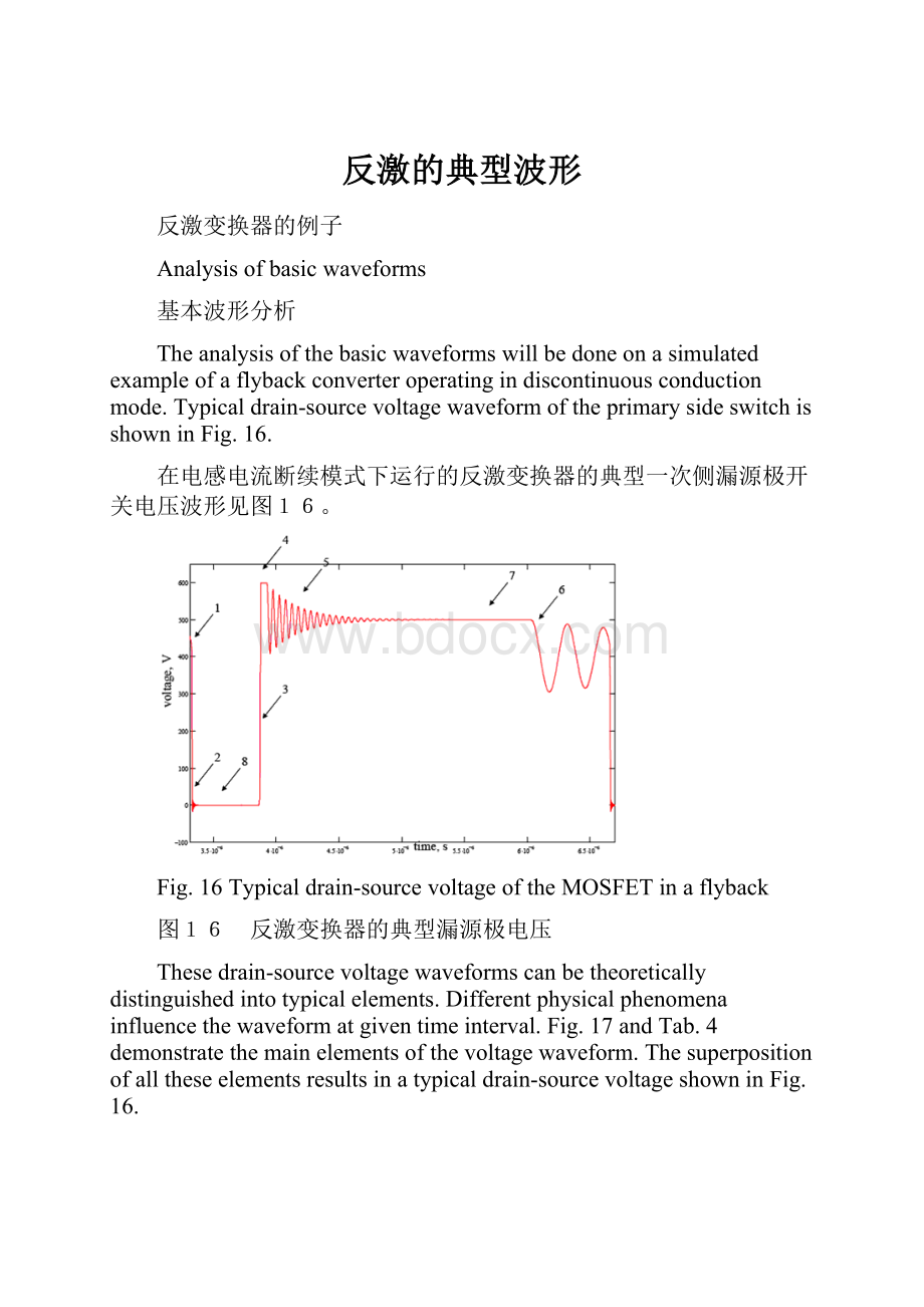
Theanalysisofthebasicwaveformswillbedoneonasimulatedexampleofaflybackconverteroperatingindiscontinuousconductionmode.Typicaldrain-sourcevoltagewaveformoftheprimarysideswitchisshowninFig.16.
在电感电流断续模式下运行的反激变换器的典型一次侧漏源极开关电压波形见图16。
Fig.16Typicaldrain-sourcevoltageoftheMOSFETinaflyback
图16 反激变换器的典型漏源极电压
Thesedrain-sourcevoltagewaveformscanbetheoreticallydistinguishedintotypicalelements.Differentphysicalphenomenainfluencethewaveformatgiventimeinterval.Fig.17andTab.4demonstratethemainelementsofthevoltagewaveform.Thesuperpositionofalltheseelementsresultsinatypicaldrain-sourcevoltageshowninFig.16.
这些漏源极电压波形能用典型的理论来描述。
各个时间段有不同物理现象影响这些波形。
图17和平台4描述了电压波形的主要原理。
把这些原理按时序整合呈现出图16所示的典型漏源极电压。
Fig.17Mainelementsofthedrain-sourcevoltage
图17 漏源极电压的主要原理
原理1:
开通期间的电压下降过程
原理2:
在开通期间因寄生震荡产生的电流尖刺
原理3:
关断期间的电压上升
原理4:
缓冲电路的钳位电压
原理5:
钳位过程结束后主要由场效应晶体管输出电容和变压器漏感引起的寄生振荡
原理6:
磁芯存储磁能释放完毕后主要由场效应晶体管输出电容和变压器电感引起的寄生振荡
原理7:
反激变换器释放磁能期间的反射电压
原理8:
与直流母线电压等幅的主要方波
Tab.4Mainelementsofthedrain-sourcevoltage
平台4 漏源极电压的主要原理
Thespectrumofthewholedrain-sourcewaveform(Fig.16)ispresentedinFig.18.
图16所示的漏源极电压呈现的电磁干扰频谱见图18。
Fig.18Spectrumofthedrain-sourcevoltage(asshowninFig.16)
图18 图16所示的漏源极电压呈现的电磁干扰频谱
Thespectraofthemainelementsofthedrain-sourcevoltagecanbefoundinFig.20.Fig.19isexactlythesameasFig.17andhasbeenrepeatedhereforbetterunder-standing.
图20描述了漏源极电压主要原理产生的电磁干扰频谱。
为便于理解,将图17映射成图19。
Fig.19Mainelementsofthedrain-sourcevoltage(repeated,sameasFig.17)
图19 漏源极电压的主要原理(正确重复 图17)
Fig.20Spectraofthemainelementsofthedrain-sourcevoltage
图20 漏源极电压主要原理产生的电磁干扰频谱
Thismethodallowsassociatingcertainpartsofthespectrumwiththeirrootcauses,i.e.thepeakat20MHzinthespectrumofthedrain-sourcevoltageiscausedbytheparasiticoscillationduetotheoutputcapacitanceoftheMOSFETandtheleakageinductanceofthetransformer.
这种方法可以确定电磁干扰频谱中某些频点的来源,也就是说漏源极电压产生的电磁干扰频谱中的20兆赫兹峰点是钳位过程结束后主要由场效应晶体管输出电容和变压器漏感引起的寄生振荡产生的。
Theanalysisofthedraincurrentoftheprimaryswitchwillbedoneinthesameway.Fig.21demonstratesatypicaldraincurrentinaDCMflyback.
对一次侧开关的漏极电流进行分析采用相同的方法。
图21展示出一个工作于电感电流断续模式反激变换器的典型漏极电流。
Fig.21Typicaldraincurrentinaflyback
图21 反激变换器的典型漏极电流
Thiswaveformcanbepresentedasasuperpositionofthefollowingelements(Fig.22andTab.5).ThesuperpositionofalltheseelementsresultsinatypicaldraincurrentshowninFig.21.
这个波形可以被看作是下列原理的叠加(图22和平台5)。
全部这些波形的叠加整合结果变成图21所示的典型漏极电流。
Fig.22Mainelementsofthedraincurrent
图22 漏极电流的主要原理
原理1:
漏极电流的主要三角波形
原理2:
在开关开通期间因寄生分布电容引起的电流尖刺
原理3:
钳位过程结束后主要由场效应晶体管输出电容和变压器漏感引起的寄生振荡
原理4:
磁芯存储磁能释放完毕后主要由场效应晶体管输出电容和变压器电感引起的寄生振荡
Tab.5Mainelementsofthedraincurrent
平台5 漏极电流的主要原理
Thespectrumofthewholedraincurrentwaveform(Fig.21)ispresentedinFig.23.
全部漏极电流波形产生的电磁干扰频谱(图21)呈现在图23。
Fig.23Spectrumofthedraincurrent(asshowninFig.22)
图23 漏极电流产生的电磁干扰频谱(与图22相同)
ThespectraofthemainelementsofthedraincurrentcanbefoundinFig.25.Fig.24isexactlythesameasFig.22andhasbeenrepeatedforbetterunderstanding.
漏极电流主要原理产生的电磁干扰频谱见图25。
图24和图22相同。
Fig.24Mainelementsofthedraincurrent
图24 漏极电流的主要原理
Fig.25Spectraofthemainelementsofthedraincurrent
图25 漏极电流主要原理产生的电磁干扰频谱
Asincaseofdrain-sourcevoltagethismethodallowstoassociatetheelementsofthedraincurrentwaveformwithitscontributiontothewholespectrum.Forexample,thepeakat20MHzinthespectrumiscausedbytheparasiticoscillationduetotheoutputcapacitanceoftheMOSFETandtheleakageinductanceofthetransformer.
就象漏源极电压的例子那样,用这种方法也可以找出漏极电流的哪一部分对电磁干扰频谱产生影响。
举例说明,20兆赫兹的峰点是钳位过程结束后主要由场效应晶体管输出电容和变压器漏感引起的寄生振荡产生的。
Thismethodofseparatingthewaveformintimedomainintoitsmainelementshelpstofindoutwhatpartofthespectruminfrequencydomaincausedbywhatrelatedphysicalphenomena.Theseparationintomainelementsshouldbedoneinrespectofreasonableeventsinthepowercircuitlikeonandoffslopes,oscillations,clamping,snubbering,reflectedvoltage,etc.
这种在时域里对主要原理进行拆分的方法有助于找出产生电磁干扰频段的干扰源。
这种离析主要原理的手法有助于合理审视电源电路里诸如变化速率、振荡、钳位、缓冲、反射电压等过程。
Inthisflybackexampleonlytheprimaryswitchhasbeenanalyzedasactivesourceofelectricalnoise.Therearealsoothers,likesecondarysidediodesorsynchronousrectifier,controlIC(especiallyitsgatedrive),etc.Inordertoobtainmorecompleteanalysisalltheseinterferencesourceshavetobeanalyzed.
在这个反激变换器里只对一次侧开关进行电磁噪声产生的分析。
但是还有其他的部分,象二次侧的二极管或同步整流器、控制集成电路(尤其是它们的栅极驱动)等等。
按顺序分析将获得更完善的关于这些电磁干扰源的解析。
However,itisimpossibletopredicttheconductedEMIspectrumusingthisapproachduetothefact,thatonlyinterferencesourcesareconsidered.Thereisnoanalysisofthespreadingpathsoftheinterferenceinthismethod.
然而,这种方法不可能预知用频谱反映的电磁干扰的实际行为,仅仅是干扰源被重视起来。
在那里没有对分布参数产生的干扰进行分析的方法。
Nevertheless,theassociationofharmonicsrootcausewiththerespectedphysicalphenomenawillreducetheeffortsofEMIreduction.Theimpactoftheidentifiedrootcausecanbereducednotonlybyfiltering,butalsobymeansofinfluencingtherootcauseitself.
不过,重视物理现象并不能成就电磁干扰的降低。
降低干扰并不仅仅是滤波,也同样意味着干扰源自身的影响。
Operationmodesofdiscontinuousflybackconverter
电感电流断续工作反激式变换器的运行模式
Theflybackconverterrunningindiscontinuousconductionmodecanbeoperatedinhardswitchingorquasiresonant(orvalleyswitching,orZVS)moderegardingtheprimarysideswitch.Thedifferencebetweenahardswitchingandquasiresonantflybackconverteristheturnontimepointoftheprimaryswitch.InahardswitchingmodetheturningonoftheMOSFETisnotsynchronizedwiththedrain-sourcevoltagevalue.Thistypeofconvertersrunsmainlyinfixedfrequencymode.
电感电流断续工作的反激式变换器一次侧开关可工作于硬开关或准谐振(或谷值开关或零电压开关)模式。
硬开关和准谐振反激变换器之间的差异在于一次侧开关的开启时间点。
在硬开关里场效应晶体管的开启波形拐点并不和漏源极电压值同步。
这种变换器大体上运行于固定频率模式。
InaquasiresonantmodetheresonantcircuitdeterminedbytheoutputcapacityoftheMOSFETandtheinductanceofthetransformerwillbeutilizedtoswitchonatlowestpossiblevalueofthedrain-sourcevoltage.Thiscircuitstartstooscillateattheendofthecurrentflowthroughthesecondarysideofthetransformer,henceattheendoftheflybackphase.TheMOSFETwillbeturnedonattheminimumofthisoscillation.ThequasiresonantapproachusesthisoscillationtoachieveminimumvoltageswitchingduringturnonfortheMOSFET.Thisoperationmoderunsatavariablefrequency.
在准谐振模式里,由变压器电感和场效应晶体管输出电容引起的谐振促使开关的开通时刻发生在漏源极电压的最小值上。
这种电路在电流从变压器二次侧流尽以后(反激回扫过程结束)开始振荡。
场效应晶体管将在振荡幅值的最小值开启(谷值开通)。
这种运行模式工作在可变的频率上。
HigheramplitudeoftheoscillationresultsinlowerdrainsourcevoltagelevelatwhichtheMOSFETturnsoncorrespondinglylowerswitchinglossesandhigherefficiencyofthesystem.
更高幅值的振荡导致场效应晶体管更低的漏源极开通电压幅值来产生更低的开关损耗和更高的系统效率。
Toachievehighoscillationpeaks,thedesignofthetransformerhastobesettohighreflectedvoltage.Thisincreaseofthereflectedvoltageresultsinahigherdrain-sourcevoltageblockingMOSFETandlongerdutycycles.
要达到比较高的振荡电压峰值,变压器的反射电压必须设置的比较高。
增加的反射电压导致使用更高漏源极击穿电压的场效应晶体管和更大的开关占空比。
Comparisonofthreedifferentflybacksolutionshasbeenmade.Allofthemhavebeenoperationat300kHz,busvoltageof400V,outputpowerof120W,outputvoltageof16V.Thesedesignincludeddifferentmodesofoperationanddifferentvaluesofreflectedvoltage,resultingindifferentMOSFET’svoltageratings:
比较现有的三种反激变换器。
它们都工作在300千赫兹,直流母线电压400伏特,输出功率120瓦特,输出电压16伏特。
这些设计包含不同的运行模式和反射电压等级,因此使用不同电压等级的场效应晶体管:
● HardswitchingflybackwithCoolMOS600V,reflectedvoltageof100V
● 硬开关反激变换器使用600伏特CoolMOS,100伏特反射电压
● QuasiresonantflybackwithCoolMOS600V,reflectedvoltageof100V
● 准谐振反激变换器使用600伏特CoolMOS,100伏特反射电压
● QuasiresonantflybackwithCoolMOS800V,reflectedvoltageof390V
● 准谐振反激变换器使用800伏特CoolMOS,390伏特反射电压
TheclampingsnubbercircuitwassettotheratedbreakdownvoltageoftheMOSFET(600Vand800Vrespectively).
钳位缓冲电路被设定在场效应晶体管的额定击穿电压上(分别为600伏特和800伏特)。
Flybackinhardswitchingmodewith600VMOSFET
使用600伏特场效应晶体管的硬开关反激变换器
Thehardswitchingapproach(asshowninFig.26)doesn’tconsidertheminimumdrain-sourcevoltage.TheMOSFETwillbeturnedonhard,inthiscaseatavoltagelevelof500V(attimepoint3.3μs).Thedischargeofcircuits’parasiticcapacitancesleadstoahighcurrentspikeduringturningon.
硬开关(图26所示)几乎不考虑漏源极电压的最小值。
场效应晶体管开通应力大,在这个例子里,开通电压在500伏特(在3.3微秒的时间点)。
由寄生电容引起的泄放电流在开通时产生很高的电流尖刺。
Fig.26Drain-sourcevoltageanddraincurrentofhardswitching600Vflyback
图26 600伏特硬开关反激变换器的漏源极电压和漏极电流
Flybackinquasiresonantmodewith600VMOSFET
使用600伏特场效应晶体管的准谐振反激变换器
Thedrain-sourcevoltage(Fig.27)startsoscillatingattheendoftheflybackphaseandreachingtheminimumof300VwhentheMOSFETturnson.
漏源极电压(图27)在反射过程结束后并减小到300伏特时场效应晶体管导通。
Thedutycycleislowercomparedtoan800Vsolutionduetoalowerreflectedvoltageof100V.Shorterdutycycleforthesameoutputpowerresultsinhigherpeakcurrentsontheprimaryside.
因为100伏特的反射电压,比较800伏特解决方案它有更小的占空比。
小占空比实现同样的功率输出必须使用更高的一次侧峰值电流。
Fig.27Drain-sourcevoltageanddraincurrentofquasiresonant600Vflyback
图27 600伏特准谐振反激变换器的漏源极电压和漏极电流
Flybackinquasiresonantmodewith800VMOSFET
使用800伏特场效应晶体管的准谐振反激变换器
Thedrain-sourcevoltage(Fig.28)startsoscillatingattheendoftheflybackphaseandreachingtheminimumof100VwhentheMOSFETturnson.Theturningoncurrentspikeislow.
漏源极电压(图28)在反射过程结束后并减小到100伏特时场效应晶体管导通。
开通电流尖刺比较低。
Thedutycycleishighercomparedtoa600Vsolutionduetoahigherreflectedvoltageof390V.Longerdutycycleforthesameoutputpowerresultsinlowerpeakcur
 升级会员
升级会员 