数字电路大型实验.docx
《数字电路大型实验.docx》由会员分享,可在线阅读,更多相关《数字电路大型实验.docx(16页珍藏版)》请在冰豆网上搜索。
数字电路大型实验
数字电路大型实验设计报告
一、实验内容
1、学习并掌握硬件描述语言VHDL
2、学习使用MAX+PLUS
3、基于EDA技术和PLD的数字系统设计
4位数字频率计的设计过程
4位数字乘法器的设计过程
4、附加内容:
30秒计时器的设计
二、数字频率计的设计
1、工作原理
频率就是周期性信号在单位时间(1S)内的变化次数。
若在一定1S的时间间隔内测得这个周期性信号的重复变化次数为N,则其频率可表示为:
F=N
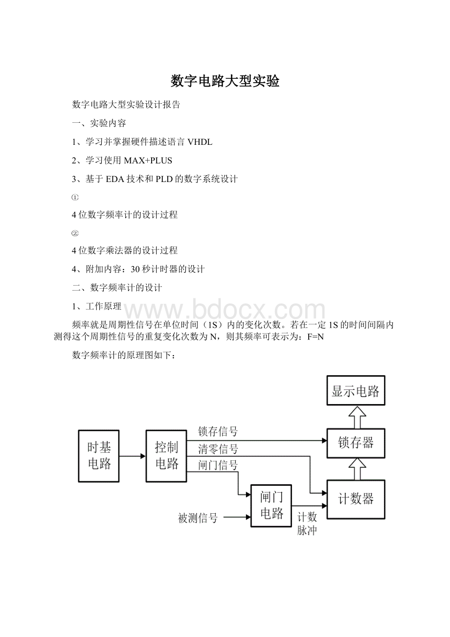
数字频率计的原理图如下:
如上图所示,当闸门信号(宽度为1S的正脉冲)到来时,闸门开通,被测信号通过闸门送到计数器,计数器开始计数,当闸门信号结束时,计数器停止计数。
由于闸门开通的时间为1S,计数器的计数值就是被测信号的频率。
为了使测得的频率值准确,在闸门开通之前,计数器必须清零。
为了使显示电路稳定地显示频率值,在计数器和显示电路之间加了锁存器,当计数器计数结束时,将计数值通过锁存信号送到锁存器。
控制电路在时基电路的控制下产生三个信号:
闸门信号、锁存信号和清零信号。
各信号之间的时序关系如下图所示:
2、数字频率计原理图
3、CNT10、CNT12、CODE、LOCK模块的VHDL语言程序
(1)CNT10的VHDL语言
libraryieee;
useieee.std_logic_1164.all;
useieee.std_logic_unsigned.all;
entitycnt10is
port(clk:
instd_logic;
clr:
instd_logic;
cs:
instd_logic;
qq:
bufferstd_logic_vector(3downto0);
co:
outstd_logic);
endcnt10;
architectureoneofcnt10is
begin
process(clk,clr,cs)
begin
if(clr='1')then
qq<="0000";
elsif(clk'eventandclk='1')then
if(cs='1')then
if(qq=9)then
qq<="0000";
else
qq<=qq+1;
endif;
endif;
endif;
endprocess;
process(qq)
begin
if(qq=9)then
co<='0';
else
co<='1';
endif;
endprocess;
end;
(2)CNT12的VHDL语言
libraryieee;
useieee.std_logic_1164.all;
useieee.std_logic_unsigned.all;
entitycnt12is
port(clk:
instd_logic;
qq:
bufferstd_logic_vector(3downto0));
endcnt12;
architectureoneofcnt12is
begin
process(clk)
begin
if(clk'eventandclk='1')then
if(qq=11)then
qq<="0000";
else
qq<=qq+1;
endif;
endif;
endprocess;
endone;
(3)CODE模块的VHDL语言
libraryieee;
useieee.std_logic_1164.all;
useieee.std_logic_unsigned.all;
entitycodeis
port(
dd:
instd_logic_vector(3downto0);
cs:
outstd_logic;
clr:
outstd_logic;
lock:
outstd_logic
);
endcode;
architectureoneofcodeis
begin
process(dd)
begin
if(dd=0)then
clr<='1';
else
clr<='0';
endif;
if(dd=11)then
lock<='1';
else
lock<='0';
endif;
if((dd>0)and(dd<9))then
cs<='1';
else
cs<='0';
endif;
endprocess;
endone;
(4)LOCK模块的VHDL语言
libraryieee;
useieee.std_logic_1164.all;
useieee.std_logic_unsigned.all;
entitylockis
port(
clk:
instd_logic;
dd:
instd_logic_vector(3downto0);
qq:
outstd_logic_vector(3downto0)
);
endlock;
architectureoneoflockis
begin
process(clk,dd)
begin
if(clk'eventandclk='1')then
qq<=dd;
endif;
endprocess;
endone;
4、CNT10、CNT12、CODE、LOCK模块的仿真结果
(1)CNT10模块的仿真结果
(2)CNT12模块的仿真结果
(3)CODE模块的仿真结果
(4)LOCK模块的仿真结果
5、项目下载步骤
(1)器件选定
选择器件为MAX7000S系列的EPM7128SLC84
(2)管脚锁定
所谓管脚锁定,就是将输入、输出信号安排在器件的指定管脚上。
在实际应用中,PLD器件常常与其它电路连在一起,因此PLD器件的管脚锁定应根据实际电路来确定。
由于本设计采用浙江工业大学电子创新基地自行研制的EDA实验板来验证设计项目,对于数字频率计应按下表来锁定引脚。
要进一步了解EDA实验板的详细情况。
信号名
管脚名
信号名
管脚名
信号名
管脚名
信号名
管脚名
LED10
64
LED20
73
LED30
4
LED40
12
LED11
65
LED21
75
LED31
6
LED41
15
LED12
67
LED22
76
LED32
5
LED42
16
LED13
68
LED23
77
LED33
8
LED43
17
LED14
69
LED24
79
LED34
9
LED44
18
LED15
70
LED25
80
LED35
10
LED45
20
LED16
74
LED26
81
LED36
11
LED46
21
CLKIN
33
CLK1
35
(3)硬件编程
使用ByteBlaster下载电缆把数字频率计项目以JATG方式下载到EDA实验板的EPM7128SLC84器件中。
在编程过程中,若器件或电缆或电源有问题,则会产生错误警告信息。
(4)频率测量
仿真结果如下:
由仿真图可知,频率测量结果正确。
三、四位乘法器的设计
1、乘法控制器的的设计
(1)乘法控制器的ASM图
(2)控制器的VHDL语言程序
libraryieee;
useieee.std_logic_1164.all;
entitymulconis
port(start,i4,bi,clk:
instd_logic;
endd,clr,ca,cb1,cb0,cm1,cm0,cc:
outstd_logic);
endmulcon;
architecturebehvofmulconis
signalcurrent_state,next_state:
bit_vector(1downto0);
constants0:
bit_vector(1downto0):
="00";
constants1:
bit_vector(1downto0):
="01";
constants2:
bit_vector(1downto0):
="11";
constants3:
bit_vector(1downto0):
="10";
begin
com1:
process(current_state,start,i4)
begin
casecurrent_stateis
whens0=>if(start='1')thennext_state<=s1;
elsenext_state<=s0;
endif;
whens1=>next_state<=s2;
whens2=>next_state<=s3;
whens3=>if(i4='1')thennext_state<=s0;
elsenext_state<=s2;
endif;
endcase;
endprocesscom1;
com2:
process(current_state,bi)
begin
casecurrent_stateis
whens0=>endd<='1';clr<='1';ca<='0';cb1<='0';
cb0<='0';cm1<='0';cm0<='0';cc<='0';
whens1=>endd<='0';clr<='0';ca<='1';cb1<='1';
cb0<='1';cm1<='0';cm0<='0';cc<='0';
whens2=>if(bi='1')thenendd<='0';clr<='1';ca<='0';
cb1<='0';cb0<='0';cm1<='1';cm0<='1';cc<='1';
elseendd<='0';clr<='1';ca<='0';cb1<='0';cb0<='0';
cm1<='0';cm0<='0';cc<='1';endif;
whens3=>endd<='0';clr<='1';ca<='0';cb1<='0';
cb0<='1';cm1<='0';cm0<='1';cc<='0';
endcase;
endprocesscom2;
reg:
process(clk)
begin
ifclk='1'andclk'eventthen
current_state<=next_state;
endif;
endprocessreg;
endbehv;
(3)控制器的仿真时序图
VHDL源程序仿真结果:
2、顶层原理图
3、顶层原理图仿真结果
四、30秒计时器设计
1、CNT3、CNT10模块的VHDL语言程序
(1)CNT3的VHDL语言
libraryieee;
useieee.std_logic_1164.all;
useieee.std_logic_unsigned.all;
entitycnt3is
port(
clk:
instd_logic;
clr:
instd_logic;
cs:
instd_logic;
qq:
bufferstd_logic_vector(3downto0)
);
endcnt3;
architectureoneofcnt3is
begin
process(clk,clr,cs)
begin
if(clr='1')then
qq<="0011";
elsif(clk'eventandclk='1')then
if(cs='1')then
if(qq=0)then
qq<="0000";
else
qq<=qq-1;
endif;
endif;
endif;
endprocess;
end;
(1)CNT10的VHDL语言
libraryieee;
useieee.std_logic_1164.all;
useieee.std_logic_unsigned.all;
entitycnt10is
port(clk:
instd_logic;
clr:
instd_logic;
cs:
instd_logic;
qq:
bufferstd_logic_vector(3downto0);
co:
outstd_logic);
endcnt10;
architectureoneofcnt10is
begin
process(clk,clr,cs)
begin
if(clr='1')then
qq<="0000";
elsif(clk'eventandclk='1')then
if(cs='1')then
if(qq=9)then
qq<="0000";
else
qq<=qq+1;
endif;
endif;
endif;
endprocess;
process(qq)
begin
if(qq=9)then
co<='0';
else
co<='1';
endif;
endprocess;
end;
2、CNT3、CNT10的仿真结果
(1)CNT3的仿真结果
(2)CNT10的仿真结果
3、计时器原理图设计
4、30秒计时器结果仿真
五、实验体会
本次数字电路大型实验让我颇有体会,不仅让我们掌握了VHDL语言和如何构建原理图,而且还让我们学会了MAX+PLUS
的使用以及如何进行结果的仿真,让我们学会了硬件电路设计的又一种新的方法,而且能够让我们每个人都亲身进行操作,增强了我们自己的动手能力,也提高了我们的学习能力,以后如果碰到硬件电路的设计,就会轻松的多,就可以用现在学过的知识运用到实践中去,不过在实验中,我也碰到了一些问题,例如,有时VHDL语言编译的时候有错误,有警告等,这时只能一处一处的找错误,有时可能是由于符号引起的错误,要特别注意。
有时在构建原理图编译时也会碰到有错误、有警告的问题,这时可能是由于原理图中线没连好的缘故,就要重新回到原理图中修改再编译,有时还要注重原理图排线的美观问题,看起来感觉比较清晰一点。
总体上来说,这次实验对我们的帮助很大,以后能够让我们更好地运用到实践中去。
 升级会员
升级会员 