使用UC3842设计的CUK降压电路无PCB电路板.docx
《使用UC3842设计的CUK降压电路无PCB电路板.docx》由会员分享,可在线阅读,更多相关《使用UC3842设计的CUK降压电路无PCB电路板.docx(20页珍藏版)》请在冰豆网上搜索。
使用UC3842设计的CUK降压电路无PCB电路板
使用UC3843设计的CUK降压电路
第一章开关电源简介
1.1开关电源原理分析
开关电源是通过脉宽调制或频率调制,控制MOS管导通时间,继而控制电感线圈的磁通量,同时又要保证电感线圈不会达到磁饱和状态,从而控制输出电压的高低。
同时通过反馈电路保证负载变化和输入电压变化时,输出电压仍能保证在一定范围内的稳定。
1.2、开关电源分类
DC/DC变换是将固定的直流电压变换成可变的直流电压,也称为直流斩波。
斩波器的工作方式有两种:
一是脉宽调制方式Ts不变,改变ton(通用);
二是频率调制方式,ton不变,改变Ts(易产生干扰)。
其具体的电路由以下几类:
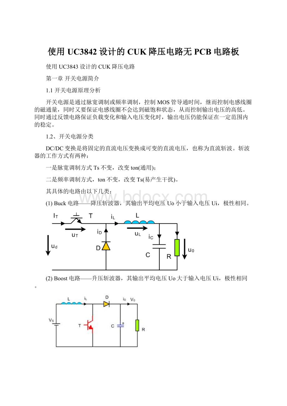
(1)Buck电路——降压斩波器,其输出平均电压Uo小于输入电压Ui,极性相同。
(2)Boost电路——升压斩波器,其输出平均电压Uo大于输入电压Ui,极性相同。
(3)Buck-Boost电路——降压或升压斩波器,其输出平均电压Uo大于或小于输入电压Ui,极性相反,电感传输。
(4)Cuk电路——降压或升压斩波器,其输出平均电压Uo大于或小于输入电压UI,极性相反,电容传输。
第二章3843设计的CUKDC-DC电路
2.1、3843性能介绍
The3842A(AM)/43A(AM)/44A(AM)/45A(AM)arefixedfrequencycurrentmodePWMcontroller.TheyarespeciallydesignedforOFF−LineandDCtoDCconverterapplicationswithaminimalexternalcomponents.Internallyimplementedcircuitsincludeatrimmedoscillatorforprecisedutycyclecontrol,atemperaturecompensatedreference,highgainerroramplifier,currentsensingcomparator,andahighcurrenttotempoleoutputideallysuitedfordrivingapowerMOSFET.Protectioncircuitryincludesbuiltundervoltagelockoutandcurrentlimiting.The3842A(AM)and3844A(AM)haveUVLOthresholdsof16V(on)and10V(off).Thecorrespondingthresholdsforthe3843A(AM)/45A(AM)are8.4V(on)and7.6V(off).TheMIK3842A(AM)andMIK3843A(AM)canoperatewithin100%dutycycle.The3844A(AM)andUC3845A(AM)canoperatewithin50%dutycycle.
The384XA(AM)hasStart-UpCurrent0.17mA(typ).
Features
•LowStart-UpandOperatingCurrent
•HighCurrentTotemPoleOutput
•UndervoltageLockoutWithHysteresis
•OperatingFrequencyUpTo300KHz(384XA)500KHz(384XAM)
2.2、引脚定义
2.3、由3843设计的CUK降压电路原理图
2.4、工作原理介绍
当+12V通过D1加到U1的第7脚后,随着电容C2两端电压慢慢升高,当电压超过8.6V时,U1开始启动,第8脚输出+5V50MA稳压电源。
同时V1也经过D1和L1给电容C1充电,C1两端的电压达到Vi,且左+右-。
第8脚输出的+5V经R1加到U1第4脚,同时为电容C3充电。
这时R1和C3组成的RC振荡电路开始工作,为U1提供稳定的工作频率。
当RC振荡进入稳态后,U1的第6脚开始输出PWM脉冲,并给R4耦合给Q1的G极。
在Ton周期,Q1导通,输入电压Vi通过L1,Q1,为电容C充电,C为负载供电。
同时C1中的电能释放,通过L2和电容C沟成回路,对电容C充电,下正上负,同时部分电能转化为磁能存储在L2中。
电源管Q1中的电流有两个,一个是L1中的电流,另一个是C1中的电流。
在Toff周期Q1截止,输入电压Vi通过L1开始为C1充电,电容C1的电压上正下负。
同时L2的电流方向不变,通过二极管D,对电容C充电,磁通转化为电能,存储在电容C中。
二极管D中有两种电流,一个是对C1的充电电流,一个L2中的电流。
所以无论Q1导通与否,C在Ton期间和Toff期间都有连续的充电电流。
(2)、状态指示
R7和LED1为指示状态设置,当-5V电压输出时,LED1亮起,说明-5V电压已经产生。
当-5V负载过重或短路时,U1保护,第6脚停止输出PWM脉冲,-5V电压消失,LED1熄灭。
(3)、过流保护
电阻R6为过流取样电阻,该电阻有两个作用,一是当该电阻上的分压大于0.8V时,U1过流保护动作,第6脚停止输出PWM脉冲,输出电压-5V消失。
二是该电阻能够对每一个方波进行检测,当通过的方波开启时间过长时,U1能够强制停止第6脚的输出,防止意外干扰导致Q1长时间导通引起过热损坏。
所以R6不能使用导线短接,否则会引起U1长时间检测不到信号,而导致Q1长时间导通而过热损坏。
(4)、输出电压调整
CUK电路的输出为负压,而UC3843的BF反馈端要求输入的电压为-0.3V—5.5V,所以直接使用电阻分压取样是不符合要求。
所以需要利用TL431和光耦配合,将负压的反馈信号转为正向电压。
R1和VR1组成反馈取样电路,调整VR1的阻值,改变VR1与R1的分压比,把此电压输出到U1的第2脚,U1改变第6脚输出的PWM占空比的大小,从而改变输出电压的高低。
2.5、元件的选用与取值
对于电感L1、L2与耦合电容C1及输出电容C8的计算,需要假定一些条件和参数不变,如下图所示
Fig2.5
WhenMOSFETQ1switcheson,therighthandsideofinductorL1isshortedtoground.Thecurrentintheinductorrampsaccordingtotheequation
whereVisthevoltageacrosstheinductor(inthiscaseitisequaltotheinputvoltage),Listheinductorvalueanddi/dtisthechangeininductorcurrentwithtime.Thuswithafixedvoltageacrosstheinductorandafixedinductorvalue,thechangeincurrentwithtimeisconstant.
WhentheMOSFETQ1switchesoff,theinductortriestomaintainitscurrentflow.Itdoesthisbycreatingavoltageacrossitwheretherighthandsidetriestoflypositive(topushcurrentoutoftherighthandend)andthelefthandsidefliesnegative.Sincethelefthandsideoftheinductorisclampedtotheinputvoltage,therighthandsideoftheinductorfliespositivetoavoltageaboveVininordertomaintaincurrentflow.TheenergyfromtheinductorflowsintocapacitorC1chargingitwithapositivevoltage(whichishigherthanVin).TherighthandsideofC1isclampedto+0.3VbydiodeD,butforthesakeofconveniencewewillignorethisvoltagedropandassumetherighthandsideofthecapacitorisclampedto0V.WewillworkoutlaterexactlywhatvoltageC1chargesto,butforthemomentitissufficienttoassumeitchargestoavoltagehigherthanVin.WewillcallthisvoltageVcap.
SincethevoltageVcapishigherthanVin,thevoltageacrosstheinductornowhastheoppositepolaritytobefore.Theinductordischargesaccordingtotheequation
whereVisthevoltageacrosstheinductor,thus
Itisinterestingtonotethatthevalueofdi/dtisdeterminedONLYbytheinductancevalueandthevoltageacrosstheinductor.ThecontrollerIChasnothingtodowithsettingtheinductorrampcurrent.
WhentheMOSFETswitchesonagainthevoltageonthedrainoftheMOSFETQ1goesfromVcapto0V.Sincethevoltageacrossacapacitorcannotchangeinstantaneously,anequalnegativegoingvoltageappearsontheanodeofdiodeDsothisnodetransitionsfrom0Vto–Vcap.Wenowhaveanegativeamplitudesquarewavevoltage(attherighthandnodeofC1)beingappliedtoanLCfilter(L2andC2).TheLCfilteraveragesoutthissquarewavetoproduceaflatDCvoltagewhoseamplitudeissomewherebetween0Vand–Vcap.Thisamplitudeisdictatedbythedutycycleofthesquarewave.
Wearenowgoingtocalculatethedutycycle(theratiooftheONtimeoftheMOSFETQ1tothetotalswitchingperiod)andthevoltage(Vcap)onthecouplingcapacitorC1.
Theinductorchargeanddischargecurrentsareequalwhenthecircuitisinsteadystate.Therefore
wheredt1istheONtimeoftheMOSFETanddt2istheOFFtimeoftheMOSFET.Dividingbothsidesby(dt1+dt2)gives
IftheDutyCycle(DC)canberepresentedby
then
so
HerewecanseetheDrainvoltagegoingfrom0VtoVcap(asyetuncalculated)andtheaccoupleddrainvoltageontheanodeofthediode.Thecapacitorhasremovedthedcoffsetandthediodehasclampedthepositiveexcursionstoroughly0V.
Now,whenthecircuitisregulatingtherewillbeaflatnegativedcvoltageontheoutput.Thus,whenV(diode)isat0VtherewillbeapositivevoltagefromV(diode)toV(out)andtheinductorcurrentinL2willrampinapositivedirection.WhenV(diode)isnegativetherewillbeanegativevoltagefromV(diode)toV(out)sotheinductorcurrentwillramptoamorenegativevalue.
Insteadystate,whentheMOSFETswitchesONV(diode)isat–VcandthevoltageacrossinductorL2is(-Vout-(-Vcap)),thusthechangeincurrentisrepresentedby
WhentheMOSFETswitchesOFF,thevoltageacrossL2is(0-(-Vout)),sothechangeincurrentisrepresentedby
Equatingthevaluesofdigives
Dividingbothsidesby(dt1+dt2)gives
whereDCisthedutycycleasdefinedabove.
Thus
Frombeforeweknowthat
So
So
Voutisthemagnitudeoftheoutputvoltage.Thisisbecauseintheabovederivation,wehaveignoredtheslopeofdi–itispositiveinL1whennegativeinL2,socannotstrictlyequatethe2statementsforDCwithoutconsideringthis.
TheresultofknowingVcapisthatwenowknowthattheDrainoftheMOSFETisexposedtoavoltageequalto(Vin+|Vout|)andhastobesizedaccordingly(asdoesthecapacitor’sworkingvoltage).
Knowingthat
and
WecanworkouttheDutyCycleintermsofVoutandVin.Thus
Again,Voutisthemagnitudeoftheoutputvoltage.
Thedutycycleissetbytheinputandoutputvoltagesonly.Theinductorvaluedoesnotfeatureinsettingthedutycycle,nordoesthecontrollerIC.
Theaboveistrueaslongasthecurrentintheinductordoesnotfalltozero.ThisiscalledContinuousConductionMode(CCM).Iftheinductorcurrentfallstozero,thedutycycleequationabovedoesnotholdandthecontrollerentersDiscontinuousConductionMode(DCM).
InCCM,iftheloadcurrentincreases,thedutycycleremainsunchanged(insteadystate).Thecircuitreactstotheincreaseinloadcurrentbykeepingthedutycycleconstant,butthemidpointoftheinductorcurrent(itsdcoffset)increases.Theswitchingfrequencyandtheamplitudeoftheinductorripplecurrentremainunchanged.
1)、IC的选择
根据设计要求和CUK电路原理计算公式,该电路输入电压12V,输出电压5V,输出电流500MA,所以可以计算出
占空比为DC==5/(5+12)=29%<50%
由于UC3843和UC3842的占空比可以达到100%,而UC3844和UC3845的占空比最高为50%。
同时UC3842和UC3844的开启电压为16V,而UC3843和UC3845的开启电压为8.4V,所以设计该电路时PWM控制IC可选择为UC3843或UC3845.
2)、InductorChoice电感L1与L2
Itisgooddesignpracticetokeeptheripplecurrentintheinductorat40%ofthetotalcurrent.Thisisagoodtradeoffbetweensmallinductorsizeandlowswitchinglosses.TheinductorontheoutputofaCukConverterisconfiguredidenticallytothatofabuckconverter.Withthebuckconverter,theaverageinductorcurrentisequaltotheoutputcurrent.Ontheinput,theCukConverterhasaninductorconfiguredidenticallytothatofaboostconverterandtheaverageinductorcurrentinaboostconverterisequaltotheaverageinputcurrent.
Withanoutputvoltageof5Vandaloadof0.5A,thisrepresentsanoutputpowerof2.5W.Allowingforanefficiencyof80%fortheconverter,thismeansourinputpowerhastobe3.125W.Withaninputvoltageof12V,thisrepresentsanaverageinputcurrentof260mA.
Iftheinputinductorcurrentrippleis40%,thenthepeakinductorcurrentis260mAx1.2,or312mAandthetroughinductorcurrentis260mAx0.8,or208mA.
Thechangeincurrentistherefore104mA.
V=12V,dt=(1/100KHZ)*29%=2.9US,
L=(12/0.104)*2.9US=33UH
Tocalculatetheoutputinductorvalue,wegothroughthesameprocedure.
Weknowthat
andweknowthevoltageontheanodeofDinFIG2.5isasquarewavewithamplitudeofVcap,weknowthattheoutputinductorhasavoltageacrossitofVcap–Vout(=Vin)whentheMOSFETisON,soforthesameONtimeouroutputinductorshouldbethesamevalueastheinputinductorforthesamechangeincurrent.Thepuristswouldarguethatsinceouroutputcurrentisdifferenttotheinputcurrentthenkeepingbothinductorvaluesthesamewillresultinadiffe
 升级会员
升级会员 