FT831B 5W demo board doc更改后.docx
《FT831B 5W demo board doc更改后.docx》由会员分享,可在线阅读,更多相关《FT831B 5W demo board doc更改后.docx(17页珍藏版)》请在冰豆网上搜索。
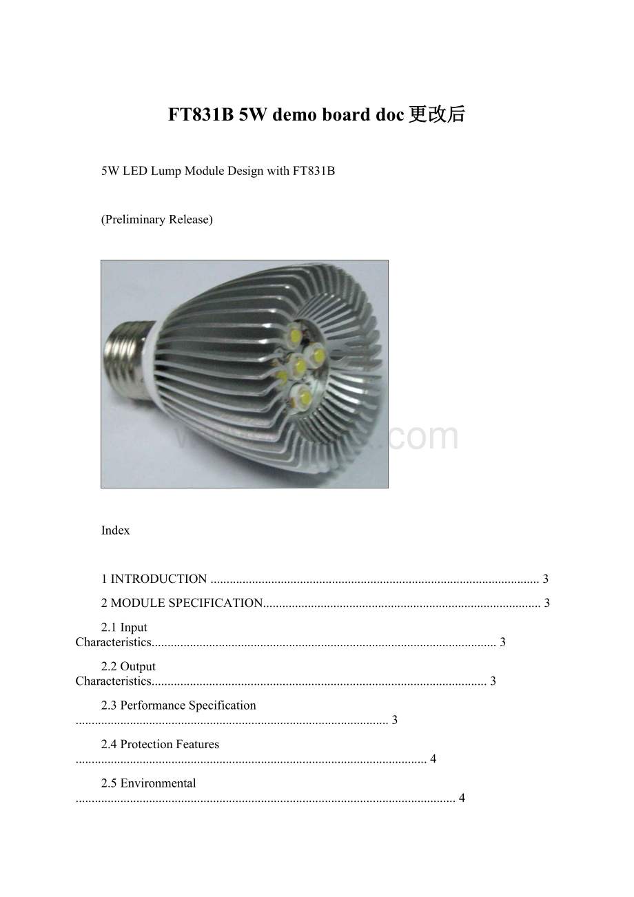
FT831B5Wdemoboarddoc更改后
5WLEDLumpModuleDesignwithFT831B
(PreliminaryRelease)
Index
1INTRODUCTION.......................................................................................................3
2MODULESPECIFICATION.......................................................................................3
2.1InputCharacteristics............................................................................................................3
2.2OutputCharacteristics.........................................................................................................3
2.3PerformanceSpecification..................................................................................................3
2.4ProtectionFeatures..............................................................................................................4
2.5Environmental.......................................................................................................................4
2.6DielectricWithstand(Hi-pot)Test......................................................................................4
2.7Insulation...............................................................................................................................4
3MODULEINFORMATION.........................................................................................5
3.1Schematic..............................................................................................................................5
3.2PCBGerber............................................................................................................................6
3.3BillofMaterials.....................................................................................................................7
3.4TransformerDesign.............................................................................................................8
1)TransformerSpecification...............................................................................................8
2)Electricaldiagram.............................................................................................................8
3)TransformerBuildDiagram.............................................................................................8
3.5ModuleSnapshot..................................................................................................................9
4PERFORMANCEEVALUATION............................................................................10
4.1InputCharacteristics..........................................................................................................11
1)InputNormalCharacteristics........................................................................................11
2)StandbyPower................................................................................................................11
4.2OutputCharacteristics.......................................................................................................11
1)PrecisionofOutputCurrent..........................................................................................11
2)Ripple................................................................................................................................11
3)TimeSequence................................................................................................................12
4.3Protection............................................................................................................................13
1)OpenCircuitProtection.................................................................................................13
2)ShortCircuitProtection.................................................................................................13
4.4EMITest...............................................................................................................................13
5SYSTEMOTHERIMPORTANTWAVEFORM........................................................15
5.1MOSFETVDSWaveformat264Vac,startup/shutdown.............................................15
5.2OutputRectifierDiodeVAKWaveformatFullLoad.....................................................15
1INTRODUCTION
ThisdocumentpresentsperformancecharacteristicsofanisolatedflybackconvertermoduledesignedwithFT831B.Themodulefeatures:
¾highprecisionforoutputcurrentinuniveralinputvoltage.
¾Simplecircuit.
Thisdocumentcontainssessionsonpowersupplyspecification,schematic/PCBGerber/BOM,transformerdesignandperformancedata.
2MODULESPECIFICATION
2.1InputCharacteristics
ACInputVoltageRating
100Vacto240Vac
ACInputVoltageRange
90Vacto264Vac
ACInputFrequency
47Hzto63Hz
Table1
2.2OutputCharacteristics
OutputVoltage
+16.4V
OutputCurrent
350mA
PrecisionofOutputCurrent
3%
RippleofOutputVoltage
2.3V
RippleofOutputCurrent
322mA
Table2
Note:
RippleofOutputVoltageismeasuredwith20MHzbandwidthlimited(peaktopeakvalue)attheendofa12-inchtwistedwireterminatedwitha10uFcapacitorinparallelwitha0.1uFceramiccapacitor.
2.3PerformanceSpecification
TotalOutputPower
5.6WTypical
StandbyPower
<0.3W@90Vac/63Hz~265Vac/47Hz,noload
Efficiency
77%min.@264Vac/50Hzwithfullload
TurnonDelayTime
≤1.1sec.max.@90Vac/50Hzwithfullload
SwitchingFrequency
45KHz±3%
Table3
2.4ProtectionFeatures
ShortCircuitProtection
Outputshutdown(AutoRecovery)
OpenCircuitProtection
OutputVoltageriseto19V
Table4
2.5Environmental
OperatingTemperature
-10℃to+40℃
OperatingHumidity
20%to90%R.H.
StorageTemperature
-40℃to85℃
StorageHumidity
0%to+90%R.H.
Table5
2.6DielectricWithstand(Hi-pot)Test
InputtoOutput3000Vac1min.
Table6
2.7Insulation
InputtoOutputDC500V10Mohmmin
Table7
3MODULEINFORMATION
3.1Schematic
Figure1:
Schematic
3.2PCBGerber
Figure2:
TopView
Figure3:
Bottomview
3.3BillofMaterials
RefDes
Description
Package
PartNum
QTY
U1
IC
SOT23-6
FT831B
1
F1
0.5A250Vac,Fuse
3.6×10mm
1
B1
0.5A600V,Bridge
SOIC-4
DB6S
1
L1
2.2mH,Inductor
4×10mm
1
Q1
1.5A700V,NPN
TO-126
13003
1
T
Transformer
EE16
1
C1,C2
4.7uF400V,Electrolytic
8×12.5mm
2
C3
470Pf250V,5%,Ceramic,X7R
0805
1
C4
100pF25V,1%,Ceramic,X7R
0805
1
C5,C6
10uF25V,5%,Ceramic,X7R
1206
2
D1
1A1000V,FastRecoveryRectifier
DO-214AC
RS1M
1
D2
1A100V,FastRecoveryRectifier
DO-219AB
RS1001FL
1
D3
2A400V,SuperFastRecoveryRectifier
DO-214AA
SS2G
1
R1,R2
560k,1/8W,5%,MetalFilm
0805
2
R3
100k,1/4W,5%,MetalFilm
1206
1
R4
27k,1/8W,5%,MetalFilm
0805
1
R5
15k,1/8W,5%,MetalFilm
0805
1
R6
3R9,1/8W,1%,MetalFilm
0805
1
R7
2,1/8W,1%,MetalFilm
0805
1
R8
0,1/8W,5%,MetalFilm
0805
1
R9
6k8,1/8W,5%,MetalFilm
0805
1
R10
200k,1/8W,5%,MetalFilm
0805
1
R11
10,1/8W,5%,MetalFilm
0805
1
Table8
3.4TransformerDesign
1)TransformerSpecification
1)Bobbin:
EE16Horizontal(10Pin)
2)CoreMaterial:
PC40(TDG).
3)L(3-1)=1700uH+/-200uH(1KHz,0.25V,25℃)
4)HI-POT:
(60Hz/5mA/3SecT).Pri.toSec.3000Vac.
2)Electricaldiagram
Figure4:
ElectricalDiagram
3)TransformerBuildDiagram
Figure5:
TransformerBuildDiagram
3.5ModuleSnapshot
Figure6:
TopView
Figure7:
bottomView
4PERFORMANCEEVALUATION
Thissessionpresentsthetestresultsof5Wmoduleuptodate.Resultsoninrushcurrent,leakagecurrentandESDarenotincludedandwillbeaddedwhentheybecomeavailable.
Overall,themodulemeetsdesignspecifications.
PerformanceHighlights:
Theefficiencyover90Vac~264Vacis≥77%
Thestandbypoweris<0.3Wat264Vac/50Hzwithnoload
CharacterizationResultsSummary
Test
Specification
Test
1.InputCharacteristics
InputVoltage
90~264V
90~264V
InputCurrent
<0.134A
Standbypower
<0.3W
0.28W
Efficiency(Average)
>73%
79%
2.OutputCharacteristics
OutputVoltageRange
15~19V
OutputCurrentRange
330~370mA
OutputVoltageRipple
2.32V
OutputVoltageRipple
0.322A
3.TimeSequence
Turnondelaytime
<3.0S
1.1S
Holduptime
6.8ms
4.Protection
OpenCircuitprotection
Pass
ShortCircuitprotection
Pass
Table9
4.1InputCharacteristics
1)InputNormalCharacteristics
Themodulewastestedatdifferentinputvoltages(from90Vacto264Vac)anddifferentloadconditions(fullloadandnoload).Efficiencyandstandbypowerweremeasuredandlistedintable10andtable11.
InputVoltage
Irms(A)
Pin(W)
Vo(V)
Io(A)
η
Specification
TestResult
90V/50Hz
0.134
7.61
16.35
0.361
77.56%
>73%
Pass
115V/50Hz
0.110
7.58
16.46
0.367
79.69%
230V/50Hz
0.073
7.55
16.35
0.372
80.56%
264V/50Hz
0.068
7.64
16.47
0.370
79.76%
Table10:
Inputcharacteristicsatfullload
2)StandbyPower
InputVoltage
Vo(V)
InputPower(W)
Specification
TestResult
90V/50Hz
18.46
0.09
<0.3W
Pass
115V/50Hz
18.54
0.09
230V/50Hz
18.79
0.21
264V/50Hz
18.76
0.28
Table11:
Standbypoweratnoload
4.2OutputCharacteristics
1)PrecisionofOutputCurrent
InputVoltage
90V
115V
230V
264V
Precision
Current
0.361A
0.367A
0.372A
0.370A
±1.5%
Table12:
PrecisionofOutputCurrent
2)Ripple
InputVoltage
90V
115V
230V
264V
RippleofOutputVoltage
2.30V
2.14V
2.16V
2.32V
Table13:
RippleofOutputVoltage
InputVoltage
90V
115V
230V
264V
RippleofOutputCurrent
0.322A
0.300A
0.300A
0.30
 升级会员
升级会员 