5V7A同步升压ZCC.docx
《5V7A同步升压ZCC.docx》由会员分享,可在线阅读,更多相关《5V7A同步升压ZCC.docx(22页珍藏版)》请在冰豆网上搜索。
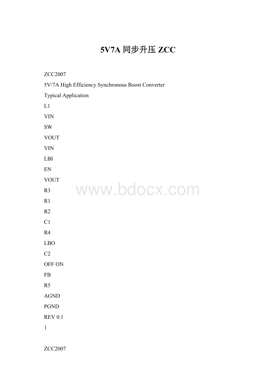
5V7A同步升压ZCC
ZCC2007
5V/7AHighEfficiencySynchronousBoostConverter
TypicalApplication
L1
VIN
SW
VOUT
VIN
LBI
EN
VOUT
R3
R1
R2
C1
R4
LBO
C2
OFFON
FB
R5
AGND
PGND
REV0.1
1
ZCC2007
ZCC2007
5V/7AHighEfficiencySynchronousBoostConverter
OrderingInformation
PartNumber*
Package
TopMarking
ZCC2007
YWLLL
ZCC2007XX
FCQFN-11(2x2mm)
*ForTape&Reel,addsuffix–Z(e.g.ZCC2007XX–Z);
PackageReference
TopView
LBI
11
VIN
10
FB
9
AGND
8
EN
1
2
7
PGND
SW
3
4
5
6
LBO
OUT
OUT
OUT
FCQFN-11(2x2mm)
(4)
(1)
ThermalResistance
FCQFN-11(2x2mm)
Notes:
θJA
80
θJC
24
AbsoluteMaximumRatings
°C/W
SW……..…..…..–0.3Vto+6V(9Vfor<5ns)
AllOtherPins...............................–0.3Vto+6V
JunctionTemperature..............................150°C
LeadTemperature...................................260°C
StorageTemp..........................-65°Cto+150°C
ContinuousPowerDissipation(TA=+25oC)
(2)
2mmx2mmFCQFN-11.............................1.56W
1)Exceedingtheseratingsmaydamagethedevice.
2)Themaximumallowablepowerdissipationisafunctionofthe
maximumjunctiontemperatureTJ(MAX),thejunction-to-
ambientthermalresistanceθJA,andtheambienttemperature
TA.Themaximumallowablecontinuouspowerdissipationat
anyambienttemperatureiscalculatedbyPD(MAX)=(TJ
(MAX)-T)/θ.Exceedingthemaximumallowablepower
dissipationwillcauseexcessivedietemperature,andthe
regulatorwillgointothermalshutdown.Internalthermal
shutdowncircuitryprotectsthedevicefrompermanent
damage.
A
JA
(3)
RecommendedOperatingConditions
SupplyVoltageVIN.......................1.8Vto5.5V
OutputVoltageVOUT......................2.5Vto5.5V
OperatingJunctionTemp.........-40°Cto+125°C
3)Thedeviceisnotguaranteedtofunctionoutsideofits
operatingconditions.
4)MeasuredonJESD51-7,4-layerPCB.
REV0.1
ZCC2007
5V/7AHighEfficiencySynchronousBoostConverter
ElectricalCharacteristics
VIN=VEN=3.3V,VOUT=5V,T=-40°Cto125°C,typicalvaluesaretestedatT=+25C,unless
A
A
otherwisenoted.
Parameter
SymbolCondition
Min
1.8
Typ
Max
5.5
1.8
Units
V
V
mV
μA
OperatingInputVoltage
UndervoltageRising
UndervoltageFalling
SupplyCurrent(Shutdown)
VIN
VINUVLO_RVINRising
VINUVLO_FVINFalling
650
0.1
IINS
VEN=0V,MeasuredatVIN
1
1
ICenabled,Noload,No
Switching,MeasuredatVIN
ICenabled,Noload,No
Switching,MeasuredatVOUT
TA=+25C
IINQ
0.3
μA
SupplyCurrent(Quiescent)
IOUTQ
FS
40
60
μA
-15%
-20%
90
600
+15%
+20%
kHz
SwitchingFrequency
-40C≤T≤125C
A
MaximumDutyCycle
ENHighThreshold
ENLowThreshold
DMAX
VENH
VENL
IEN
95
%
V
V
VENRising(micropower)
VENFalling(micropower)
ConnectedtoVIN
1.0
0.4
ENInputLeakageCurrent
0.1
800
800
1
0.3
808
812
50
μA
TA=+25C
792
788
FeedbackVoltage
VFB
IFB
mV
nA
-40C≤T≤125C
A
FeedbackleakageCurrent
High-sideMOSFET
On-resistance
Low-sideMOSFET
On-resistance
VFB=0.85V
RONH
20
20
mΩ
RONL
mΩ
LinearChargeCurrent
Limit
SWCurrentLimit(5)
OutputOvervoltage
ProtectionThreshold
VOUT=0V
VOUT=1.7V
0.2
1
ILIM_LN
ILIM_SW
VOVP
A
A
V
(5)
7
5.6
5.7
5.8
LBIThreshold
VLBI
VLBIfalling
490
500
510
mV
LBIHysteresis
VLBIhys
ILBI
10
mV
μA
V
LBILeakageCurrent
LBOLowThreshold
V=VorGND
0.1
0.3
0.3
EN
IN
VLBO
VOUT=3.3V,ILBO=100μA
0.4
LBOLeakageCurrent
ThermalShutdown
ThermalShutdown
ILBO
TSD
VLBO=5.5V
0.1
150
μA
C
TSDhys
25
C
Hysteresis
Notes:
5)Guaranteedbycharacterization,notproductiontested.
REV0.1
3
ZCC2007
5V/7AHighEfficiencySynchronousBoostConverter
PinFunctions
Package
Pin#
NameDescription
1
EN
Enablepinofthechip.Thispinmustnotbefloatingbutterminated.
PowerSwitchOutput.SWisconnectedtotheinternalmainswitchandsynchronous
switch.
2
3
SW
LBOLowbatterycomparatoroutput(opendrain)
Boostconverteroutputpin.VOUTiscompletelydisconnectedfromVINwhenENis
low.
4,5,6
VOUT
7
8
PGNDPowerGround.
AGNDAnalogGround.
FeedbackInput.ConnectingaresistordividerfromVOUTtothispintoadjustVOUT
voltage.ThispinmustbeconnectedtoVOUTonfixedVOUTvoltageversion.
9
FB
10
11
VINInputSupplyPin.VINmustbelocallybypassed.
LBILowbatterycomparatorinput(comparatorenabledwithEN)
REV0.1
4
ZCC2007
5V/7AHighEfficiencySynchronousBoostConverter
startmechanismpreventshighinrushcurrent
fromtheinputpowersupply.
OPERATION
TheZCC2007isahighefficiencysynchronous
boostconverterwithtrueoutputdisconnect.
Thedevicefeaturesfixedfrequency(600kHz)
current-modePWMcontrolforexcellentline
andloadregulation.Integratedlowon-
resistancepowerswitches,combiningwith
frequencystretchingandpowersavemode
(PSM)atlightloads,improvetheefficiencyover
awideloadrange.Internalsoft-startandloop
compensationsimplifiesthedesignprocessand
minimizesthenumberofexternalcomponents.
PWMandPSM
TheZCC2007automaticallyenterspowersave
mode(PSM)whentheloaddecreasesand
resumespulsewidthmodulation(PWM)mode
whentheloadincreases.InthePWMmode,at
thebeginningofeachcycle,theinternalN-
channelMOSFETswitchisturnedon,forcing
theinductorcurrenttorise.Thecurrentofthis
switchisinternallymeasuredandconvertedto
avoltagebythecurrentsenseamplifier.That
voltageiscomparedtotheoutputvoltageofthe
erroramplifier.Whenthesetwovoltagesare
equal,thePWMcomparatorturnsoffthe
internalN-channelMOSFETswitchandforces
theinductorcurrentflowingintotheoutput
capacitorthroughtheinternalP-channel
MOSFETswitch.Thiscausestheinductor
currenttodecrease.Thepeakinductorcurrent
iscontrolledbyVCOMP,whichinturnis
controlledbytheoutputvoltage.Thusthe
outputvoltageisregulatedthroughtheinductor
currenttosatisfytheload.InthePSM,the
devicelowerstheswitchingfrequencyandthen
switchestopulseskipmodeiftheloaddrops
EnableandDisable
ThedeviceisenabledbysettingENpinhigh
(>1.2V).WhenENpinispulledtoground,the
deviceisdisabled,switchingisstoppedandall
internalcircuitryisturnedoff.Theoutputis
isolatedfromtheinput.
Start-up
Afterthedeviceisenabled,theinternal
referenceandbiascircuitsareactivatedwhen
therisingVINtripstheunder-voltagelockout
threshold(VINUVLO_R).
Atfirst,the
rectifierturnsontochargetheoutputcapac
linearlyinlinearchargemode.Thedeviceexit
linearchargemodewhentheoutputischarged
to1.7V.Inlinearchargemode,thePMOS
chargingcurrentisbeingregulatedtoavoid
inrushcurrentandlimittheoutputcurrent
duringshort-circuitprotection(SCP).
chargingcurrentisproportionaltotheoutput
voltage,whichis0.2Awhentheoutputis0V
andrampsto0.7Awhentheoutputis1.7V.
Oncetheoutputreaches1.7V,thedevicestarts
switchingandtheoutputslowlyrampsuptothe
targetedvalueinsoft-start.
downMode
ncasethatthetargetedVoutislowerthan
+0.3V,theZCC2007operatesinastep-down
modewithalowerpeakcurrentlimitthanthatin
up(boost)mode.Inthisstep-downmode,
theoperationissimilartothatinthePWM
modeexceptthatthegateofinternalP-channel
MOSFETistiedtoVIN.
CurrentLimit
Toavoidanaccidentallargepeakcurrent,an
internalcycle-by-cyclecurrentlimitoperationis
adopted.Theinternallysensedinductorcurrent
isconvertedtoavoltageandcomparedtothe
peakcurrentlimit.TheinternalN-channel
MOSFETswitchisturnedoffimmediatelyas
soonastheinductorcurrentreachesthelimit.If
theloadcurrentisfurtherincreasedandthe
outputispulledbelowtheinputvoltage,the
SoftStart(SS)
Inlinearchargemode,thesoft-startvoltage
followsthevoltageonFBpin.Asthedevice
startsswitching,thesoft-startvoltageisrising
slowlybycharginganinternalcapacitorwitha
currentsource.Thereferencevoltagerisesat
thesamerateofsoft-startvoltage.Thesoft-
startendswhenthesoft-startvoltagereaches
0.8V.Thetypicalsoft-starttimeis2ms.Soft-
REV0.1
5
ZCC2007
5V/7AHighEfficiencySynchronousBoostConverter
ZCC2007entersintoshortcircuitprotection(SCP)
mode.
belowauser-setthresholdvoltage.The
functionisactiveonlywhenthedeviceis
enabled.Whenthedeviceisdisabled,theLBO
pinishigh-impedance.Theswitchingthreshold
is500mVatLBI.Duringnormaloperation,LBO
staysathighimpedancebecausethevoltageat
LBIisabovethethreshold.Itbecomesactively
lowwhenthevoltageatLBIgoesbelow00
mV.
ShortCircuitProtection
Onceshortcircuitprotection(SCP)istriggered,
theZCC2007stopsswitchingimmediatelyand
restartsafterabout1msasanewpower-on
cycle.Thedevicecontinuesthishiccupsteady
stateuntiltheoverloadconditionisremoved.
Thebatteryvoltage,atwhichthedetection
circuitswitches,canbeprogrammedwitha
resistivedividerconnectedtotheLBIpin.The
resistivedividerscalesdownthebatteryvoltage
toavoltagelevelof500mV,whichisthen
comparedtotheLBIthresholdvoltage.TheLBI
pinhasabuilt-inhysteresisof10mV.Seethe
applicationsectionformoredetailsaboutthe
programmingoftheLBIthreshold.Ifthelow-
batterydetectioncircuitisnotused,theLBIpin
shouldbeconnectedtoGND(ortoVBAT)and
theLBOpincanbeleftunconnected.Donotlet
theLBIpinfloat.
OutputDisconnect
Whenthedeviceisshutdown,theZCC2007
disconnectsVOUTfromVINbyeliminating
bodydiodeconductionoftheinternalP-channel
 升级会员
升级会员 